1. The Evolution of CPO and the Thermal Bottleneck of Microring Modulators
The explosive growth of AI computing clusters and the evolution of data center interconnection rates to 100Gbps/lane and above have driven the transformation of Co-Packaged Optics (CPO) technology from concept to large-scale deployment. Its core value lies in breaking the traditional discrete architecture of “optical module + motherboard” and co-packaging optoelectronic chips on the same substrate, which reduces interconnection loss by more than 60% and power consumption by 30%, making it the core cornerstone for supporting ultra-high-speed AI Interconnect and high-density communication scenarios. Microring Modulators (MRMs) have become the core optoelectronic devices of CPO optical engines due to their micro-scale size, ultra-high modulation efficiency, and natural compatibility with Wavelength Division Multiplexing (WDM) technology. However, constrained by the intrinsic material properties and the extreme thermal environment of CPO packaging, temperature stability has become a key bottleneck restricting the release of their performance. Resonant wavelength drift caused by the thermo-optic effect and waveguide structural deformation due to thermal expansion will directly damage modulation contrast and channel isolation, ultimately leading to system bit error rate (BER) exceeding the tolerance threshold.
Unlike the relaxed thermal environment of traditional pluggable optical modules, the high-density integration, high power concentration, and compact layout characteristics of CPO Advanced Packaging put forward subversive requirements for the temperature stability design of microring modulators. It is necessary to achieve in-depth breakthroughs from four dimensions: the essence of the thermal environment, device mechanism, packaging adaptation, and system collaboration, rather than simply applying traditional temperature control schemes. From the perspective of industrial practice, the current technical route selection of silicon photonics CPO modulators also confirms the core position of temperature stability. Mainstream schemes include silicon photonics MZM (Mach-Zehnder Modulator) structures, silicon photonics microring structures, etc. Although MZMs have better temperature stability, their large size makes them difficult to adapt to the high-density integration needs of CPO. Microring modulators have become the preferred choice of leading enterprises such as TSMC and NVIDIA due to their small size, but their strong temperature sensitivity needs to be compensated by designs such as built-in heaters. This further highlights the necessity of the “multi-dimensional temperature control design” idea.
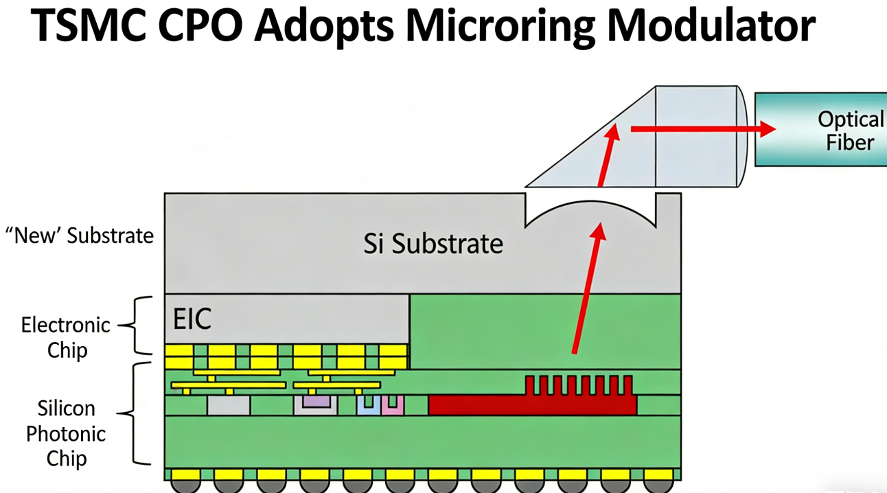
This diagram illustrates the core structure of TSMC’s Co-Packaged Optics (CPO) technology, which integrates an electronic chip and a silicon photonic chip into a single package, using a microring modulator to convert electrical signals into optical signals at high speed.
The bottom layer features solder ball pins for external connections. The green silicon photonic chip layer contains the red microring modulator, which receives electrical signals and generates optical signals. The gray electronic chip layer (EIC) drives and controls the silicon photonic chip, while the top silicon substrate provides physical support and interconnection.
Optical signals generated by the microring modulator are coupled into an optical fiber via an angled structure, enabling ultra-high-speed, low-power optical connections between computing chips and external devices, and resolving the bandwidth bottleneck of traditional electrical signal transmission.
2. The Essence of CPO Thermal Environment: High Density and Thermal Crosstalk
Compared with the deployment mode of traditional optical modules with independent heat dissipation and physical isolation from electrical chips, the core contradiction of CPO packaging lies in the coupling problem of “concentrated thermal load and limited thermal diffusion paths brought by high-density integration”. Its thermal environment is not a linear conduction of a single heat source, but a complex system with multiple heat sources, multiple paths, and strong coupling: switching chips (heat flux density up to 1000W/cm² or more), acceleration chips (XPU) and optical engines (single-channel power consumption 5-10mW, array-level up to tens of watts) are densely arranged on the same high-speed substrate (such as silicon interposer, organic substrate).
Heat forms three-dimensional thermal accumulation through substrate conduction, inter-chip radiation, and intra-cavity convection, resulting in the junction temperature of the optical engine area being generally 15-25℃ higher than that of traditional modules. More importantly, the compact design of CPO packaging (substrate size usually in the order of tens of millimeters) makes thermal crosstalk present the characteristics of “near-field strong coupling and far-field superposition” — the distance between the driver circuit, photodetector and microring modulator inside the optical engine is only hundreds of microns. Local heating will form a micro-scale thermal gradient, and the temperature difference between microrings of different channels can reach 5-8℃, which is far exceeding the 2-3℃ tolerance threshold of traditional modules. This directly causes the imbalance of multi-channel wavelength consistency and brings fatal interference to the WDM system.
3. Process Adaptation and Structural Innovation: From RDL to Substrate Optimization
From the perspective of industrial process practice, the thermal environment pain points of CPO packaging have directly promoted the collaborative optimization of packaging technology and device design, which is clearly reflected in the Heterogeneous Integration technical routes of enterprises such as TSMC, ASE Technology, and Shenghe Jingwei, and is highly consistent with the core idea of “precision temperature control + thermal field balance”. The previously discussed ASE CPO scheme and Shenghe Jingwei’s glass substrate CPO 3D packaging process (Y11T359) both adopt traditional RDL (Redistribution Layer) technology. Their dielectric materials are organic polymers such as PI, and the interlayer vias are called plastic vias or organic TDV (Through Dielectric Via) — such dielectric vias have extremely small parasitic capacitance due to their insulating properties, which can meet the bandwidth requirements of CPO high-speed transmission. This forms a core difference from TSV (Through Silicon Via): TSV will generate semiconductor-oxide-metal MOS parasitic capacitance due to its silicon semiconductor material, which seriously restricts bandwidth performance.
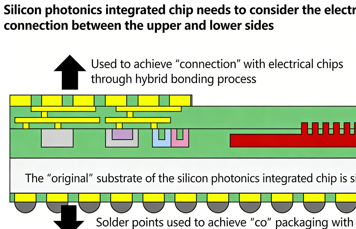
This diagram illustrates the vertical interconnection and system integration design of a silicon photonic integrated chip. Its core lies in enabling collaborative operation with external circuits through electrical connections on both the upper and lower sides: the upper side is directly connected to the driving electrical chip via hybrid bonding technology, while the lower side achieves co-packaging with the application-specific integrated circuit (ASIC) through solder bumps. While this structure enhances signal transmission efficiency, it also presents significant thermal management challenges. The silicon substrate, as the foundation of the chip, serves both as a platform for optoelectronic devices and a critical pathway for heat conduction. Generally speaking, using a liquid cooling plate as the base plate for cooling is a relatively high-efficiency approach.High-density integration and high-frequency, high-speed signal processing generate substantial heat inside the chip. If this heat cannot be effectively dissipated through the substrate and packaging structure, it will cause performance drift and reduced reliability of the optoelectronic devices. Therefore, thermal management is a core element throughout the design of such silicon photonic integrated chips, from chip architecture to packaging implementation, and must be optimized in conjunction with the upper and lower interconnection schemes to ensure stable system operation under high loads.
However, traditional organic polymer dielectrics have obvious shortcomings: they are easy to decompose at high temperatures, and have a large coefficient of thermal expansion (CTE), which is prone to delamination and cracks, bringing hidden dangers to the reliability of microring modulators working under long-term heating conditions. Based on this, in its CPO silicon photonics integration scheme (referring to materials such as TSMC’s OFC2025 silicon photonics packaging speech Y11T96 and silicon photonics COUPE assembly vertical coupling structure Y11T151), TSMC innovatively avoids traditional PI resin RDL vias and TSV vias, and optimizes the structural design for the high-temperature resistance needs of high-speed microring modulators: its transmitter adopts microring modulators, and one of the core measures is to remove the original silicon substrate of the silicon photonics integrated chip. Combined with the vertical coupling assembly structure (Y11T151), it adapts to the design needs of built-in heaters above the microrings, reduces thermal accumulation and thermal stress from the process level, ensures the reliability of materials under long-term heating conditions, and at the same time takes into account bandwidth optimization (Y11T299) and power consumption control (Y12T14, Y11T323).
4. Multi-Dimensional Thermal Control: Active Cooling, Layout, and Reliability Standards
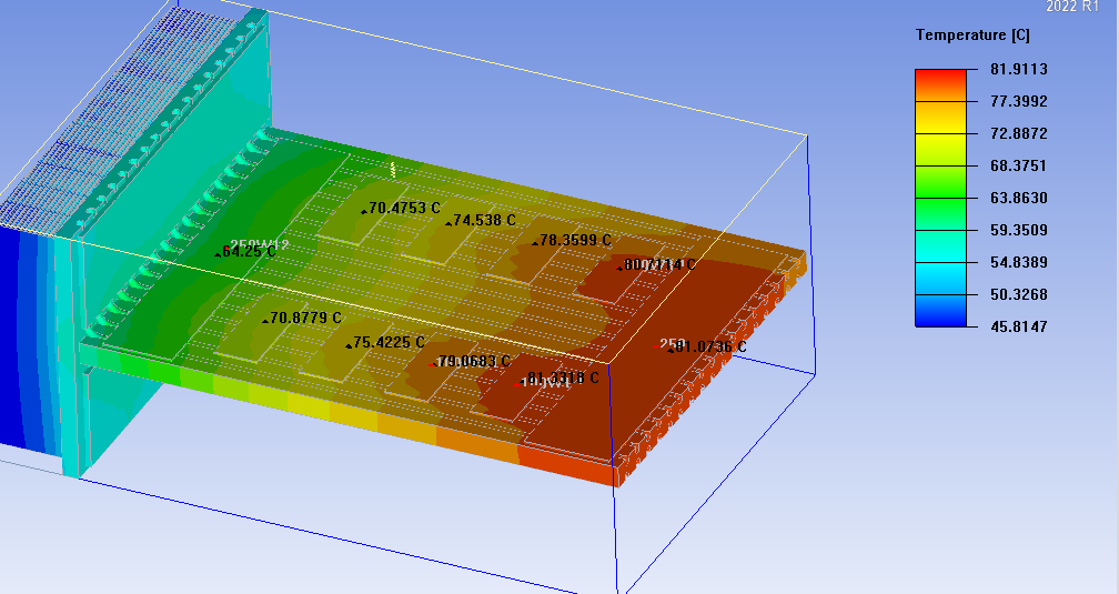
This is a typical landing case of the “packaging process adaptation to thermal environment” idea, and a critical step in CPO Thermal Management. The core to solve this pain point is to break the traditional thinking of “passive heat dissipation + simple isolation” and build an active design system of “precision temperature control + thermal field balance”. First, to address the problem of surging heat density, it is necessary to adopt a “hierarchical heat dissipation + directional heat conduction” scheme. For example, deploy a microchannel liquid cooling structure under high-power electrical chips to quickly export core heat through forced convection of liquid working fluid, and at the same time equip an ultra-thin vapor chamber in the optical engine area to control the local junction temperature fluctuation of the microring modulator within ±1℃.
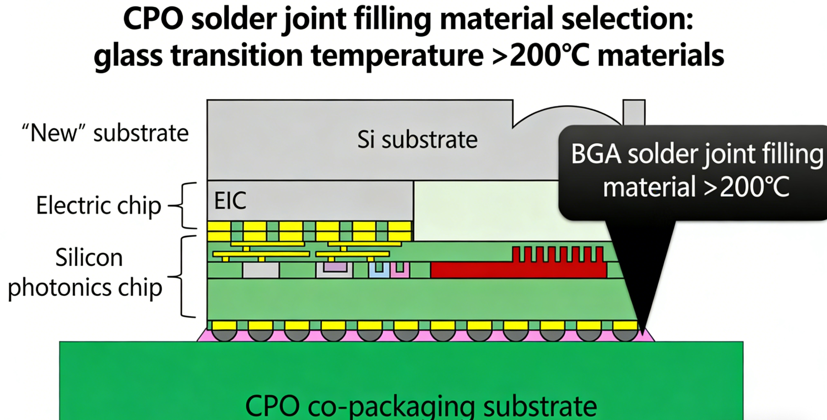
This diagram illustrates the core structure of CPO (Co-Packaged Optics), with a key design requirement that the glass transition temperature (Tg) of the BGA solder joint underfill material must be >200°C. This requirement directly supports the core goal of CPO thermal management. From the cross-sectional view, the CPO consists of a Si substrate, electrical chip (EIC), silicon photonic chip, and co-packaging substrate, with each layer connected electrically and mechanically via BGA solder joints. Due to its high integration and power density, the heat flux of CPO is far higher than that of traditional packaging, leading to sustained high-temperature environments during operation and manufacturing, which imposes stringent challenges on thermal reliability. The selection of underfill materials with Tg >200°C is precisely to meet this thermal management need. Such materials maintain structural rigidity at high temperatures, mitigating stress caused by thermal expansion mismatch between different materials, and preventing solder joint deformation and fatigue failure due to thermal cycling. This supports long-term stable operation in high-speed optical communication scenarios and is a critical component for ensuring thermomechanical reliability in the CPO thermal management system.
Second, optimize the substrate thermal layout and thermal isolation design, build a thermal field distribution model based on finite element thermal simulation (such as ANSYS Icepak), arrange the microring array in the thermal neutral zone of the substrate, block the heat conduction path from high-power chips to microrings through thermal isolation grooves (width ≥200μm) and low thermal conductivity media (such as aluminum nitride ceramic gaskets), and control the distance between microrings to be ≥100μm to reduce inter-channel thermal crosstalk. Third, establish CPO packaging thermal threshold management and control standards, and clarify the upper limit of the optical engine operating junction temperature ≤45℃ and the inter-channel temperature difference ≤3℃ in combination with the microring temperature drift characteristics and system transmission requirements, so as to avoid the impact of the thermal environment on microring performance from the source.