Have you ever stopped to think about the silent revolution happening all around us? It’s in the smooth, instant acceleration of an electric vehicle, the seamless flow of energy from a solar panel into the grid, and the tireless precision of an industrial robot. A single, unsung hero working behind the scenes—a powerful electronic switch—makes these incredible feats of modern technology possible. This component is the gatekeeper of energy, controlling massive electrical currents with microscopic precision. Understanding this device isn’t just an academic exercise; it’s the key to unlocking the next generation of power efficiency and innovation, in a market that Statista projects will be worth nearly $5 billion by 2025.
An Insulated Gate Bipolar Transistor (IGBT) is a high-power semiconductor device that merges the simple gate-drive control of a MOSFET with the high-current, low-loss capability of a bipolar transistor. Its primary function is to act as an extremely efficient switch, managing huge flows of electrical power with minimal energy waste. This hybrid design makes it an indispensable component in modern electric vehicles, renewable energy inverters, and industrial motor drives, enabling a more powerful and sustainable technological future.
But how did this small component become the powerhouse behind our green energy transition and transportation revolution? And more importantly, how do you navigate its complexities to choose, test, and implement the right one for your project? This guide is your ultimate 2025 resource, designed to answer those questions and more. We will take you on a journey from the IGBT’s invention in the 1980s to its cutting-edge applications in Silicon Carbide (SiC) and Gallium Nitride (GaN) technology today. Whether you’re a seasoned engineer designing a next-generation inverter, a student of electronics, or a tech enthusiast curious about what powers our world, we’ll break it all down. Let’s switch on the power and dive in.
The History and Evolution of IGBT Technology
Dr. Jayant Baliga invented the Insulated Gate Bipolar Transistor (IGBT) at General Electric in the early 1980s, creating a revolutionary hybrid of MOSFET and BJT technologies. Its history features key milestones, including commercialization in the 1980s, high-voltage advancements in the 1990s, and the shift from planar to trench gate structures. This evolution has dramatically improved efficiency and power handling, making the IGBT a cornerstone of modern power electronics.
Origins of the IGBT
To truly appreciate the IGBT, you have to understand the problem engineers designed it to solve. In the late 1970s, power electronics engineers faced a frustrating trade-off. They had the MOSFET, which was fast and easy to control, but inefficient at high voltages. They also had the BJT, which handled high power well but was slow and difficult to drive. Engineers wanted the best of both worlds. This challenge led to the groundbreaking work of Dr. Jayant Baliga, who patented the IGBT in 1982. His invention brilliantly combined the input structure of a MOSFET with the output structure of a BJT into a single device, creating a component that could switch high power with the simplicity engineers dreamed of.
Key Milestones in IGBT Development
The journey from a patent to a global industry standard was a rapid one, with continuous innovation from companies like Toshiba and Fuji Electric. Each decade brought significant advancements:
- 1980s – Commercialization: The first commercial IGBTs hit the market, proving the technology’s viability in motor drives and setting the stage for future growth.
- 1990s – The Rise of High Voltage: This decade saw the development of more rugged Non-Punch-Through (NPT) IGBTs, pushing voltage ratings higher and expanding their use into demanding industrial and traction applications.
- 2000s – The Efficiency Revolution: The introduction of Trench Gate and Field-Stop (FS) structures dramatically lowered energy losses, enabling higher power density and paving the way for more compact devices.
- 2010s to 2025 – The Wide-Bandgap Era: The focus has shifted to new materials like Silicon Carbide (SiC) and Gallium Nitride (GaN), allowing IGBTs to operate at higher temperatures and frequencies with even lower losses.
From Early Devices to Modern Innovations
The evolution from planar (flat) to trench (vertical) gate structures was a pivotal moment. This architectural change allowed for a much higher cell density within the silicon, which had a massive impact on performance.
This structural shift wasn’t just an incremental improvement; it was a fundamental redesign that slashed energy losses by allowing more current to flow through a smaller area. This directly translated to less wasted heat, higher power density, and paved the way for the compact inverters in today’s EVs and solar arrays.
Historical Context and Inventors
While Dr. Baliga is the primary inventor, the IGBT’s development was a global effort. Here is a simplified timeline of its evolution:
| Year/Era | Key Milestone | Impact on Technology |
|---|---|---|
| 1982 | Dr. Jayant Baliga files the patent for the IGBT. | Created the first high-power switch with low drive power. |
| 1990s | Development of more rugged NPT-IGBTs. | Expanded use in high-reliability industrial applications. |
| 2000s | Trench Gate & Field-Stop structures become standard. | Drastic reduction in energy losses, enabling higher power density. |
| 2025+ | Integration of SiC and GaN wide-bandgap materials. | Pushing efficiency and speed limits for EVs and renewables. |
How Does an IGBT Work? Detailed Operating Principles
An IGBT uses a small voltage at its insulated gate to control a large current flow between its collector and emitter terminals. The internal MOSFET structure provides easy voltage control, which in turn activates the internal BJT structure, allowing for high current conduction with a very low on-state voltage drop (Vce(sat)). This hybrid operation combines the best features of both technologies, enabling efficient, high-power switching with minimal control effort.

Fundamental Working Mechanism
At its heart, the IGBT operates like a sophisticated, electronically controlled valve for electricity. The magic lies in how its two internal components work in harmony. Applying a positive voltage (typically +15V) to the Gate terminal relative to the Emitter creates an electric field across the silicon dioxide layer. This field forms a conductive “channel” in the silicon, just like in a standard MOSFET. This channel allows a small initial current to flow, which then acts as the base current to turn on the main power-handling part of the device—the BJT. Once the BJT is activated, it opens the floodgates, allowing a massive current to flow from the Collector to the Emitter with very little resistance. To turn it off, you simply remove or reverse the gate voltage; the channel disappears, cutting off the BJT’s base current and stopping conduction.
Switching Modes: On-State and Off-State
An IGBT has two primary states of operation, and its ability to transition between them rapidly is what makes it so useful.
- On-State (Conduction): When the gate-emitter voltage (Vge) exceeds the threshold voltage (Vge(th)), the IGBT is fully on. In this state, it acts like a closed switch, with a very low voltage drop across it, known as the saturation voltage or Vce(sat). A low Vce(sat) is crucial because it minimizes conduction losses (Power Loss = Vce(sat) × Collector Current), which means less wasted energy and less heat.
- Off-State (Blocking): When the gate voltage is zero or negative, the IGBT is off and acts like an open switch. It can block very high voltages across its collector and emitter terminals with minimal leakage current. Early IGBTs faced a phenomenon called “latch-up,” where the internal thyristor-like structure could get stuck in the on-state, but modern designs have virtually eliminated this risk.
V-I Characteristics and Curves
Engineers use characteristic curves to understand and predict how an IGBT will behave in a circuit. The most important is the output characteristic, which plots the collector current (Ic) against the collector-emitter voltage (Vce) for different gate voltages. This graph clearly shows the device’s “safe operating area” (SOA)—the combination of voltage and current where it can operate without damage. It also visualizes the low Vce(sat) value in the active region, confirming its low conduction losses. The formula Vce(sat) = f(Ic) highlights that the on-state voltage drop is a function of the current passing through it, a critical parameter for thermal design.
Switching Dynamics: Turn-On and Turn-Off
The transition between on and off is not instantaneous and is where most of the energy loss occurs in high-frequency applications. When an IGBT turns off, it exhibits a “tail current”—a small, lingering flow of current that slowly decays. Minority charge carriers in the BJT part of the device taking time to clear out cause this phenomenon, which is a primary source of switching loss (Eoff).
Managing these switching dynamics is one of the biggest challenges in high-frequency inverter design. The tail current and the Miller effect—a parasitic capacitance that slows down switching—are the main culprits behind energy loss and heat generation. Innovations like Field-Stop layers and advanced gate driver circuits are specifically designed to minimize these effects, pushing efficiency higher.
Switching losses can account for 10-20% of the total energy loss in an IGBT, so minimizing them is key to building efficient systems. This is why faster-switching SiC and GaN devices are becoming so important for next-generation applications.
Thermal and Electrical Behavior
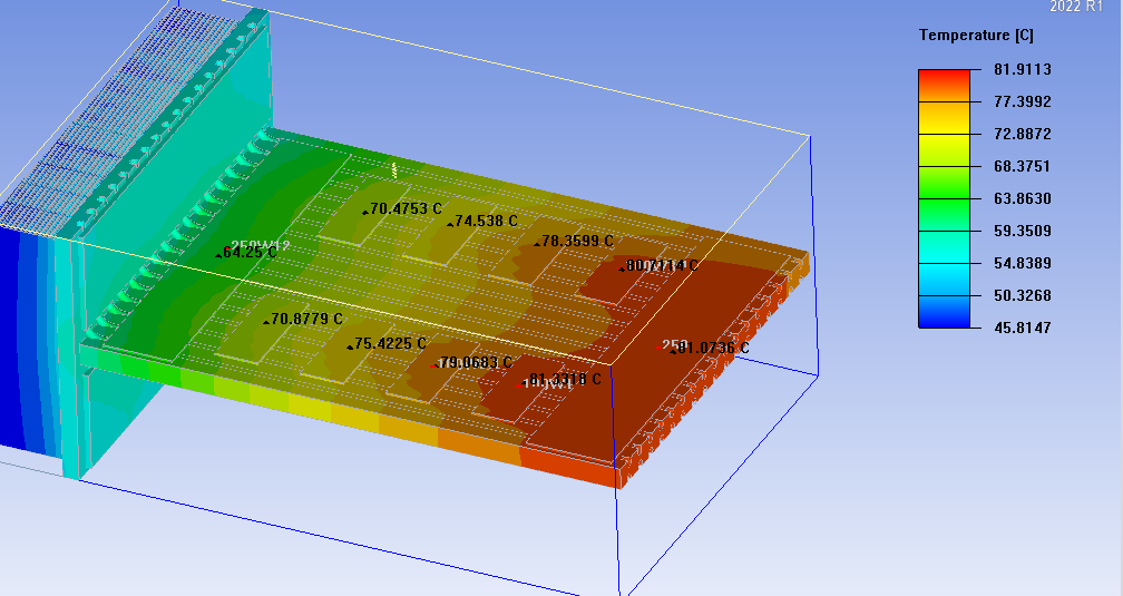
Heat is the ultimate enemy of any semiconductor. An IGBT’s performance is highly dependent on its junction temperature (Tj), which engineers must typically keep below 150°C or 175°C. As the temperature rises, its on-state voltage can increase, leading to more power loss and more heat—a dangerous cycle known as thermal runaway. This is why effective thermal management is non-negotiable. For high-power applications, engineers often connect multiple IGBT chips in parallel inside a single module to share the current load. This requires careful matching of the chips and a robust thermal design to ensure heat is drawn away evenly from all of them.
Types of IGBTs: Classifications and Variants
Not all IGBTs are created equal. To meet the diverse demands of modern electronics, engineers create them in several different types, primarily classified by their internal structure, voltage rating, and the semiconductor material used. Choosing the right type is a critical design decision that balances performance, ruggedness, and cost for a specific application, from a simple home appliance to a high-performance electric vehicle.

Based on Structure
The physical construction of an IGBT has the biggest impact on its performance characteristics. The main structural types you’ll encounter are:
- PT-IGBT (Punch-Through): This is one of the original IGBT structures. It features an N+ buffer layer that helps reduce the on-state voltage and switching time, making it relatively fast. However, it has a symmetrical blocking capability, which is not needed for most applications, and is more complex to manufacture.
- NPT-IGBT (Non-Punch-Through): A more robust and thermally stable design that is easier to manufacture. NPT-IGBTs are known for their ruggedness and positive temperature coefficient, which makes them easy to parallel. They are slower than PT types but are workhorses in many industrial applications.
- Trench-IGBT: The modern standard for high performance. By creating a vertical gate in a “trench,” this structure dramatically increases the channel density. This results in a significantly lower on-state voltage (Vce(sat)) and therefore much lower conduction losses, making it the preferred choice for high-efficiency applications.
Based on Voltage Rating
Engineers segment IGBTs by the maximum voltage they can safely block, which aligns them with different application tiers:
- Low-Voltage (<600V): These are often found in consumer electronics and automotive applications like electric power steering where power requirements are moderate.
- Medium-Voltage (600V – 1700V): This is the most common range, covering everything from industrial motor drives and solar inverters to the traction inverters in mainstream electric vehicles.
- High-Voltage (>1700V): Reserved for heavy-duty applications like high-speed trains, wind turbines, and grid-level power transmission (HVDC systems).
Based on Material
While silicon is the traditional material, the industry is rapidly moving towards wide-bandgap semiconductors for the next leap in performance.
The transition from Silicon (Si) to Silicon Carbide (SiC) is arguably the most significant innovation in power electronics today. SiC-based power devices can operate at higher temperatures, block higher voltages in a smaller die size, and switch significantly faster with lower losses. For the electric vehicle industry, this means smaller, lighter, and more efficient inverters, which directly translates to longer range and faster charging.
Specialized and Emerging Variants in 2025
Beyond the main categories, several specialized IGBTs exist to solve specific problems. Field-Stop (FS) IGBTs are a popular modern variant that adds a special layer to drastically reduce the tail current, cutting down on switching losses. Reverse-Conducting (RC) IGBTs integrate an anti-parallel diode onto the same chip, saving space and cost in compact inverter designs. Looking ahead to 2025 and beyond, we are seeing the rise of GaN (Gallium Nitride) hybrids, which promise even faster switching speeds for applications like high-frequency power supplies and renewable energy systems.
Summary of IGBT Types
| Classification | Key Characteristics | Pros | Cons | Approx. Cost/Unit |
|---|---|---|---|---|
| NPT-IGBT | Rugged, symmetrical structure | Robust, easy to parallel | Slower, higher Vce(sat) | $5 – $20 |
| Trench-FS IGBT | High cell density, low losses | Very low Vce(sat), fast | More complex manufacturing | $10 – $35 |
| SiC-Hybrid IGBT | Silicon Carbide material | High temp, ultra-fast, efficient | Significantly higher cost | $25 – $50+ |
IGBT Characteristics: Electrical, Thermal, and Performance Metrics
To properly design with IGBTs, engineers must become fluent in the language of their datasheets. These documents contain critical metrics that define how the device will behave under different conditions. Understanding these electrical, thermal, and performance characteristics is the key to creating a circuit that is not only functional but also efficient, reliable, and safe. We can broadly divide these metrics into two categories: how the device behaves when it’s holding steady (static) and how it behaves when it’s switching (dynamic).
Static Characteristics
These parameters describe the IGBT’s performance in a stable, unchanging state—either fully on or fully off.
- Saturation Voltage (Vce(sat)): This is arguably the most important static metric. It’s the small voltage drop across the collector and emitter when the IGBT is fully on. A lower Vce(sat) (typically 1V to 2.5V) means lower conduction losses and less heat generation, which is crucial for overall system efficiency.
- Threshold Voltage (Vge(th)): This is the minimum gate-emitter voltage required to turn the IGBT on. It’s typically in the range of 4V to 6V. Knowing this value is essential for designing the gate driver circuit to ensure the IGBT turns on reliably without being susceptible to noise.
Dynamic Characteristics
These metrics describe how the IGBT behaves during the transition between on and off states. In high-frequency applications, these characteristics are often the dominant source of power loss.
- Switching Times (t_on, t_off): These values, which we measure in nanoseconds (ns), define how quickly the IGBT can turn on and off. Typical values range from 100ns to over 500ns. Faster switching times are generally better as they reduce the time the device spends in the high-dissipation transition phase.
- Switching Energy Losses (E_on, E_off): Datasheets quantify the energy the device loses during each turn-on and turn-off event. These losses are directly proportional to the switching frequency—the faster you switch the IGBT, the more energy you lose per second. Calculating these losses is critical for thermal design.
Thermal Management is Non-Negotiable
An IGBT converts every watt of lost energy, whether through conduction or switching, directly into heat. Managing this heat is the single most important factor in ensuring the device’s long-term reliability.
The key thermal metric on any datasheet is the Junction-to-Case Thermal Resistance (Rth(j-c)). This value tells you how effectively heat can travel from the active silicon chip (the junction) to the outside of the component’s package (the case). A lower Rth(j-c) is always better. However, this is only half the battle; an effective heat sink is required to move that heat from the case to the ambient air, keeping the junction temperature within its safe operating limit.
Reliability and Lifetime
Modern IGBTs are incredibly reliable, with a Mean Time To Failure (MTTF) often exceeding one million hours under specified operating conditions. However, their lifespan can be significantly shortened if they are pushed beyond their limits. High-voltage IGBTs used in applications like high-speed rail or grid infrastructure also face unique challenges, such as the risk of failure from cosmic rays—high-energy particles from space that can strike the silicon and cause catastrophic breakdown. Manufacturers design and test for these events to ensure maximum reliability.
Performance in Real-World Circuits
Beyond the datasheet numbers, real-world performance depends on the surrounding circuit. When paralleling multiple IGBTs to handle higher currents, it’s crucial that they have closely matched characteristics, especially Vge(th) and Vce(sat), to ensure they share the current evenly. Furthermore, all high-power IGBT circuits must include robust protection features. This includes short-circuit protection to shut the device down safely during a fault condition and the use of derating curves, which guide engineers on how much to reduce the maximum allowable current and voltage as the operating temperature increases.
Advantages and Disadvantages of IGBTs
Like any feat of engineering, the IGBT is a masterclass in trade-offs. Its unique hybrid design gives it a powerful set of advantages that make it the dominant choice in high-power electronics, but it also comes with inherent limitations that designers must understand and mitigate. Acknowledging both sides of the coin is crucial for selecting the right component and designing a truly optimized system.
Key Advantages
The reasons for the IGBT’s widespread adoption are clear and compelling. They offer a combination of features that no other single device could previously match.
- High Power Capability: Manufacturers build IGBTs to handle serious power, with ratings that can go up to 6500V and 3000A. This makes them ideal for applications like EV traction inverters and utility-scale solar converters.
- Low Conduction Losses: Thanks to their BJT-like output, IGBTs have a very low on-state voltage drop (Vce(sat)). This means less energy is wasted as heat when the device is conducting high currents, leading to superior system efficiency.
- Simple Gate Drive: The MOSFET input stage means IGBTs are voltage-controlled devices. They require very little current to turn on, which dramatically simplifies the gate driver circuitry compared to the complex, power-hungry circuits needed for BJTs.
- Good Switching Speed: While not as fast as a MOSFET, an IGBT offers a “sweet spot” of switching speed (typically 1-20 kHz) that is fast enough for most high-power applications, providing a great balance between speed and power handling.
Disadvantages and Limitations
Despite its strengths, the IGBT is not without its drawbacks. These limitations are often the deciding factor in choosing a different component, like a MOSFET, for a specific application.
- Higher Switching Losses than MOSFETs: The BJT structure that gives the IGBT its low conduction loss also causes the infamous “tail current” during turn-off. This phenomenon leads to higher switching losses, which become more significant as the operating frequency increases.
- Slower Switching Speed: Compared to a pure MOSFET, an IGBT is a slower device. This makes it unsuitable for very high-frequency applications like the power supplies found in modern computers and servers, which often operate in the hundreds of kHz.
- Risk of Thermal Runaway: Although modern designs are much better, some IGBTs can exhibit a negative temperature coefficient under certain conditions, where their resistance decreases as they get hotter. This can cause one device in a parallel array to hog current, get even hotter, and eventually fail.
The Engineer’s Trade-Off
Choosing an IGBT is a balancing act. The engineer must weigh the need for low conduction losses and high voltage capability against the switching losses that come with higher frequencies. For an EV inverter, the low on-state loss is paramount for efficiency during acceleration. For a high-frequency power supply, a MOSFET’s lower switching loss is the winning factor. The “best” device is always dictated by the application’s unique demands.
Designers often employ clever strategies to mitigate these disadvantages. For example, using “soft-switching” techniques in the circuit can significantly reduce the switching losses, allowing the IGBT to be used at higher frequencies than would otherwise be practical. This kind of system-level design is where true engineering innovation happens.
Summary: IGBTs vs. Alternatives
| Feature | IGBT | Power MOSFET | Real-World Impact |
|---|---|---|---|
| Voltage Range | High (600V – 6500V) | Low to Medium (<1000V) | IGBTs are essential for connecting solar farms to the grid. |
| Conduction Loss | Very Low (Low Vce(sat)) | Low, but increases with voltage | Using IGBTs in EV inverters can improve range by 5-10%. |
| Switching Speed | Medium (1 – 50 kHz) | Very High (>200 kHz) | MOSFETs are required for compact, high-frequency phone chargers. |
| Control Circuit | Simple (Voltage Driven) | Simple (Voltage Driven) | Both are much easier to control than older BJT technology. |
IGBT vs. Other Power Devices: MOSFET, BJT, and Thyristor Comparisons
While the IGBT is a dominant force in power electronics, it doesn’t operate in a vacuum. To truly understand its place, an engineer must compare it against the other key players in the semiconductor world: the speedy MOSFET, the classic BJT, and the high-power Thyristor. Each device has a specific arena where it excels, and choosing the right one is a matter of matching the component’s strengths to the application’s demands for voltage, current, speed, and control.
IGBT vs. MOSFET
This is the most common and critical comparison in modern power design. It’s a classic battle between high-voltage brawn and high-frequency speed.
- Application Domain: The clearest dividing line is voltage. MOSFETs are the undisputed champions at lower voltages (typically below 600V). Engineers use them in countless applications like computer power supplies, Class-D audio amplifiers, and low-voltage motor controllers. IGBTs, on the other hand, are designed to take over where MOSFETs leave off, excelling in high-voltage applications from 600V up to several kilovolts.
- Conduction vs. Switching Loss: At high voltages, a MOSFET’s on-state resistance (RDS(on)) becomes prohibitively high, leading to massive conduction losses. An IGBT, with its low, fixed saturation voltage (Vce(sat)), is far more efficient in this regard. However, the roles reverse when it comes to switching. A MOSFET can turn on and off almost instantaneously with minimal loss, while an IGBT’s “tail current” creates significant switching losses, making MOSFETs the only choice for very high-frequency designs.
IGBT vs. BJT
This comparison is more of a look back in time, as engineers specifically invented the IGBT to replace the BJT, and it has done so in almost all new designs.
The core difference is in the control mechanism. A BJT operates as a current-controlled device, meaning it requires a continuous, high-power current into its base to stay on. An IGBT, with its MOSFET front-end, operates as a voltage-controlled device. This allows engineers to drive it with simple, low-power circuits, making it vastly more efficient and easier to integrate into modern digital control systems.
IGBT vs. Thyristor/SCR
When it comes to handling truly massive amounts of power (thousands of amps and volts), the Thyristor (or Silicon-Controlled Rectifier, SCR) is still king. However, it comes with a major limitation in control.
- Control Capability: An IGBT offers full control; you can turn it on and off at will with the gate signal. A Thyristor, on the other hand, can only be turned on. Once it starts conducting, it will remain “latched on” until the main current flowing through it drops to zero.
- Application Suitability: This latching behavior makes Thyristors ideal for simple, phase-controlled applications like AC power controllers or high-power rectifiers. However, it makes them completely unsuitable for the high-frequency, variable-duty-cycle switching required by modern inverters. For any application that uses Pulse-Width Modulation (PWM) to control power—like a motor drive or solar inverter—the IGBT is the superior choice.
When to Choose an IGBT Over Others
So, where is the IGBT’s sweet spot? It is the go-to device for applications that fall into this specific window:
- High Voltage (>600V)
- High Current (>50A)
- Medium Switching Frequency (1 kHz to 50 kHz)
This combination perfectly describes the operating conditions found in electric vehicle powertrains, industrial motor drives, large-scale solar inverters, and uninterruptible power supplies (UPS). In these areas, the IGBT provides an unbeatable blend of power handling, efficiency, and controllability.
A Head-to-Head Comparison
| Parameter | IGBT | Power MOSFET | Thyristor (SCR) |
|---|---|---|---|
| Voltage Rating | High (up to 6.5kV) | Low-Medium (up to 1kV) | Very High (up to 12kV) |
| Current Rating | High (up to 3kA) | Medium (up to 200A) | Very High (up to 5kA) |
| Switching Frequency | Medium (1-50 kHz) | Very High (>200 kHz) | Very Low (<1 kHz) |
| Control Method | Voltage (Full On/Off) | Voltage (Full On/Off) | Current (Turn-On Only) |
| Typical Application | EVs, Solar Inverters | DC-DC Converters, SMPS | HVDC, Phase Control |
Common Applications of IGBTs in Modern Technology
The IGBT’s unique blend of high power handling and efficient control has made it the backbone of countless modern technologies. From the factory floor to the open road, and from renewable energy farms to the appliances in our homes, IGBTs are the invisible force managing the flow of electrical power. Their versatility allows them to operate across a vast spectrum of applications, each with its own unique set of challenges and demands.
Power Electronics and Inverters
This is the IGBT’s home turf. An inverter’s job is to convert DC power to AC power, and an IGBT’s ability to switch high currents on and off rapidly makes it perfect for the task. The most prominent example is the Variable Frequency Drive (VFD), which engineers use in industrial automation. By using IGBTs to vary the frequency of the AC power supplied to a motor, a VFD can precisely control the motor’s speed. This has a massive impact on energy efficiency, often cutting a motor’s energy consumption by 20-30% or more. Similarly, Uninterruptible Power Supplies (UPS) rely on IGBTs to instantly switch from grid power to battery power during an outage, protecting critical systems like data centers and hospitals.
Renewable Energy Systems
IGBTs power the green energy revolution. In a solar energy system, photovoltaic panels generate DC electricity. A solar inverter, built around a core of high-voltage IGBTs, converts this DC power into grid-compatible AC power. In large, utility-scale solar farms, these inverters handle megawatts of power (1-10MW), a task for which IGBT modules are uniquely suited. Likewise, wind turbines generate variable-frequency AC power, which must be converted to DC and then inverted back to grid-frequency AC. This complex power conversion process relies entirely on the high-power switching capability of IGBTs.
Electric Vehicles and Transportation
Perhaps the most visible and exciting application for IGBTs today is in the electric vehicle (EV). The traction inverter is the heart of an EV’s powertrain, responsible for converting the DC power from the battery pack into the AC power that drives the electric motor. This process happens thousands of times per second, demanding incredible efficiency and reliability. The performance of the IGBTs directly impacts the vehicle’s range, acceleration, and overall performance. Leading automakers like Tesla have pushed this technology even further by adopting advanced SiC-based power modules to gain a competitive edge in efficiency.
Beyond passenger cars, IGBTs are also the workhorses in public transportation, powering the traction systems in high-speed trains, trams, and electric buses, where their ability to handle thousands of volts and amps is essential.
Industrial and Consumer Applications
The reach of the IGBT extends into a surprising number of everyday applications. High-power welding machines use IGBTs to create high-frequency inverters that allow for smaller, lighter, and more controllable welders. Induction heating systems, used for everything from industrial metal forging to the cooktop in your kitchen, rely on IGBTs to generate the high-frequency magnetic fields needed to heat materials without direct contact. Even some high-end home appliances, like microwave ovens and air conditioners, use IGBT-based inverters for more precise and efficient power control.
High-Power and Emerging Uses in 2025
Looking to the future, IGBTs are becoming critical components in upgrading our global energy infrastructure. They enable High-Voltage Direct Current (HVDC) transmission systems, which transport massive amounts of power over long distances with lower losses than traditional AC lines. As our power grids become “smarter,” engineers will use IGBTs in devices like solid-state transformers and grid-tied energy storage systems to manage power flow with unprecedented speed and flexibility. As of 2025, we are also seeing increased adoption in the power supplies for AI data centers, where energy efficiency is a top-tier priority.
Summary of Common IGBT Applications
| Sector | Specific Application Examples | Typical Power Range | Key Benefit of Using IGBTs |
|---|---|---|---|
| Electric Vehicles | Traction Inverters, On-Board Chargers | 50kW – 250kW | High efficiency for longer range, high power density. |
| Renewable Energy | Solar Inverters, Wind Turbine Converters | 5kW – 10MW+ | Reliable high-voltage handling, high conversion efficiency. |
| Industrial | Motor Drives (VFDs), Welding, UPS | 1kW – 1MW+ | Precise control, energy savings, and ruggedness. |
| Transportation | High-Speed Trains, Electric Buses | 500kW – 5MW+ | Extreme reliability and very high power handling. |
Testing, Control, and Safety Considerations for IGBTs
Deploying an IGBT in a high-power system is more than just dropping it into a circuit. To ensure a design is reliable, efficient, and safe, engineers must rigorously test the component, implement sophisticated control strategies, and build in multiple layers of protection. Overlooking any of these steps can lead to suboptimal performance at best, and catastrophic failure at worst. This is where the practical side of engineering comes into play, moving from theoretical datasheets to real-world application.
How to Test IGBTs
Before putting an IGBT into service, and especially when troubleshooting a faulty circuit, engineers need to test it. While a dedicated curve tracer is the professional’s tool for characterizing a device, a simple digital multimeter can perform a basic health check.
- Using a Multimeter (Diode Mode): A quick and easy test can check for the most common failure: a short circuit. By using the diode check function, you can test the integrity of the internal body diode between the emitter and collector. You should see a forward voltage drop in one direction and an open circuit in the other. You can also check for a gate-to-emitter or gate-to-collector short, which would indicate a failed device.
- In-Circuit Testing: For more detailed analysis, an oscilloscope is essential. By probing the gate voltage and the collector current simultaneously, engineers can measure actual switching times, observe the tail current, and check for issues like voltage overshoots or ringing, which can indicate problems in the circuit layout or gate driver.
Gate Drive Circuits and Control Strategies
The gate driver is the “brain” that tells the IGBT when to turn on and off. A well-designed gate driver is critical for performance and protection.
A proper gate drive isn’t just about applying a voltage; it’s about applying the *right* voltage, with the *right* amount of current, at precisely the *right* time. The driver must supply a stable voltage (typically +15V to turn on and 0V or a negative voltage to turn off) with enough peak current to charge and discharge the IGBT’s input capacitance quickly. Slow or weak gate drive leads to slow switching, which dramatically increases energy losses and thermal stress.
Modern gate drivers also incorporate crucial protection features. One of the most important is desaturation protection, which constantly monitors the IGBT’s on-state voltage (Vce(sat)). If the voltage suddenly rises while the device is supposed to be on (a sign of a short circuit), the driver will immediately and safely shut the IGBT down before it can destroy itself.
Safety and Protection Features
Given the immense power they control, a robust ecosystem of safety features must surround IGBTs. These include:
- Overcurrent Protection: Engineers can implement this through the gate driver (desaturation protection) or with external sensors to shut the system down if the current exceeds a safe limit.
- Overtemperature Protection: Engineers often place a temperature sensor (like an NTC thermistor) directly on the IGBT module’s baseplate. If the temperature exceeds a preset limit, the system will either throttle back the power or shut down completely.
- Snubber Circuits: These are small networks of resistors and capacitors placed across the IGBT to suppress the large voltage spikes that can occur during high-speed switching, protecting the device from avalanche breakdown.
Common Failure Modes and Prevention
Understanding why IGBTs fail is key to preventing it. The most common failure modes are avalanche breakdown (caused by overvoltage), thermal runaway (caused by inadequate cooling), and latch-up (an older issue now largely designed out). The number one prevention strategy is to always respect the device’s Safe Operating Area (SOA) by following derating guidelines. This means operating the IGBT well below its maximum rated voltage, current, and temperature to ensure a long and reliable service life.
Future Trends and Innovations in IGBT Technology
The world of power electronics never stands still, and the IGBT is at the forefront of this constant evolution. As we look towards 2025 and beyond, several key trends are shaping the future of this powerhouse component. The relentless push for greater efficiency, higher power density, and improved reliability is driving innovation in materials, integration, and design, ensuring the IGBT remains essential for decades to come.
Advancements in Materials: The SiC and GaN Revolution
The most significant trend is the move beyond silicon. Wide-bandgap semiconductors are set to redefine the limits of performance.
- Silicon Carbide (SiC): SiC is rapidly becoming the material of choice for high-performance applications. Its ability to operate at higher temperatures, voltages, and frequencies with lower losses makes it a perfect fit for the demanding environment of EV inverters. According to IDTechEx, the market for SiC in EVs is expected to surge past $10 billion by the end of the decade, a testament to its game-changing potential.
- Gallium Nitride (GaN): While SiC excels at high voltages, GaN is the champion of speed. GaN-based devices can switch orders of magnitude faster than silicon, enabling a new generation of ultra-compact, high-frequency power supplies and renewable energy micro-inverters.
Integration and Intelligent Power Modules (IPMs)
The future lies in integration. Instead of using discrete IGBTs, designers are increasingly turning to Intelligent Power Modules (IPMs). These modules combine the IGBTs, freewheeling diodes, and sophisticated gate driver and protection circuits into a single, optimized package.
Using an IPM simplifies the design process, reduces component count, and improves reliability by ensuring all the critical components are perfectly matched and thermally managed. It’s a system-in-a-box approach that accelerates development time and shrinks the overall footprint of the power conversion system.
Sustainability and Efficiency Improvements
As the world focuses on sustainability, the efficiency of power conversion becomes paramount. Every fraction of a percent of energy saved in an IGBT translates to massive energy savings on a global scale. Future research will continue to focus on reducing both conduction and switching losses to push inverter efficiencies ever closer to the theoretical limit of 100%. Furthermore, as power modules become more common, the industry is also developing initiatives for recycling and refurbishing these complex components to reduce electronic waste.
2025 Outlook: Challenges and Research Directions
The path forward is not without challenges. The primary obstacle for wide-bandgap materials like SiC and GaN remains cost, although prices are falling rapidly as manufacturing scales up. Thermal management also becomes even more critical; as devices become smaller and more powerful, the challenge of extracting waste heat intensifies, driving demand for advanced cooling solutions like liquid cold plates. Looking ahead, researchers are even exploring the use of AI and machine learning to optimize the internal structures of IGBTs and predict their lifetime in real-world conditions, opening up a new frontier in power semiconductor design.
Frequently Asked Questions
- What is an IGBT?An IGBT, or Insulated Gate Bipolar Transistor, is a semiconductor switch that combines the easy voltage control of a MOSFET with the high-power capability of a BJT. Engineers use it to efficiently control large amounts of electrical power.
- What is the main function of an IGBT?Its main function is to act as a high-speed, high-power electronic switch. It turns large currents and voltages on and off with very little energy loss, making it ideal for inverters, motor drives, and power supplies.
- What is the difference between an IGBT and a MOSFET?The main difference is their application range. MOSFETs are best for low-voltage (<600V), high-frequency applications. IGBTs are superior for high-voltage (>600V), high-current applications where low conduction losses are more important than ultra-fast switching.
- What are the advantages of IGBTs?Their key advantages are high voltage and current handling, very low on-state power loss (conduction loss), and a simple, low-power gate drive circuit, which makes them easy to control.
- What are IGBTs used for?Engineers use them in electric vehicles, solar and wind energy inverters, industrial motor controls (VFDs), welding machines, uninterruptible power supplies (UPS), and high-speed trains.
- What is the difference between an IGBT and a thyristor?You can turn an IGBT on and off at will with its gate signal. A thyristor (SCR) can only be turned on; it remains latched on until the main current stops flowing, making it unsuitable for high-frequency switching applications.
- How do you test an IGBT?You can do a basic test with a multimeter in diode mode to check for shorts between the terminals and to verify the integrity of the internal body diode. For detailed analysis, an oscilloscope is needed to measure its switching characteristics.
Conclusion
From its conceptualization as a “best of both worlds” solution to its current position as a pillar of the green energy and transportation sectors, the Insulated Gate Bipolar Transistor has proven to be one of the most impactful inventions in modern electronics. It is the component that makes high-power, high-efficiency energy conversion not just possible, but practical. As technology continues to evolve with advanced materials like SiC and greater integration in Intelligent Power Modules, the IGBT will become even more critical in our pursuit of a more sustainable and electrified future.
Understanding the principles, characteristics, and applications of the IGBT is no longer just for power electronics specialists; it’s essential knowledge for any engineer or innovator working on the cutting edge of technology. The challenges of tomorrow will demand even more from these components, especially in the realm of thermal management where every watt of lost energy must be effectively dissipated.
If your project demands the highest levels of power efficiency and reliability, the right thermal solution is just as critical as the right semiconductor. At Kenfa Tech, we specialize in creating custom, high-performance cooling solutions—from advanced skived fin heat sinks to liquid cold plates—engineered to unlock the full potential of your IGBT-based designs. Contact our experts today for a consultation and let us help you solve your most demanding thermal challenges.