
1. Introduction
With the continuous iteration of semiconductor chip manufacturing processes and the rapid upgrading of computing power, the power density of high-end chips has increased significantly. Traditional planar heat dissipation structures are limited by fixed heat exchange area, long heat conduction paths and high heat loss, which can hardly adapt to high-load and high-heat-flux operating scenarios. Consequently, common problems including chip heat accumulation, frequency reduction and insufficient operational stability have become increasingly prominent.In the post-Moore era, Huawei proposed the Tau (τ) three-dimensional hierarchical architecture, which breaks the traditional planar chip design mindset. Its core principle is to shorten signal transmission paths and reduce transmission loss through three-dimensional stacking and hierarchical layout, improving overall operational efficiency without relying solely on advanced process shrinking. Based on this innovative design concept, KENFA TECH has innovatively developed a double-layer stacked liquid cooling plate heat dissipation structure. This design migrates the core advantages of three-dimensional layering, transmission path shortening and loss reduction to the field of chip thermal management, effectively solving the heat dissipation bottleneck of high-power-density chips.
2. Pain Points of Traditional Heat Dissipation Structures for High-Power Chips
At present, mainstream chip heat dissipation solutions mostly adopt planar single-layer liquid cooling plates and vapor chambers. For conventional chip heat sources with a contact area of 60×60mm, such planar structures have obvious technical shortcomings. Firstly, the fixed heat exchange area of single-layer structures cannot provide sufficient heat exchange margin for high-heat-flux concentrated heat generation of high-power chips, resulting in slow heat diffusion. Secondly, the planar layout only supports unidirectional heat conduction and single coolant heat exchange path, leading to long heat conduction distance and high overall thermal resistance. Thirdly, planar heat dissipation structures have low space utilization and cannot fully exploit the heat dissipation potential within limited installation space. Under high-load working conditions, the core temperature of the chip remains high, severely restricting the peak performance and long-term operational stability of the chip.
3. Design and Core Principle of Double-Layer Stacked Liquid Cooling Structure
Abandoning the traditional planar heat dissipation design, the double-layer stacked liquid cooling plate structure independently developed by KENFA TECH fully draws on the core design concepts of Huawei’s Tau architecture, including three-dimensional layering, multi-dimensional efficiency improvement and transmission path shortening, realizing structural optimization of the chip heat dissipation system and perfectly matching the heat dissipation requirements of high-power-density chips.
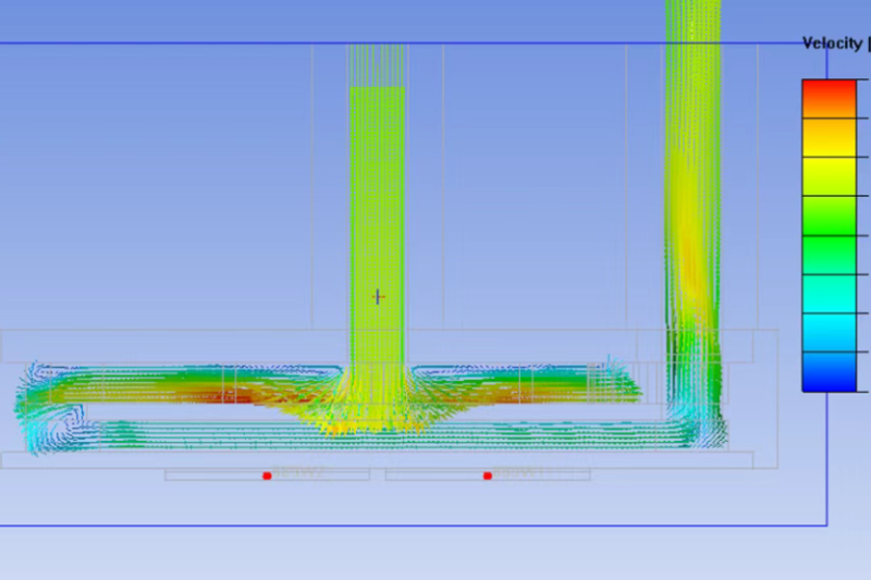
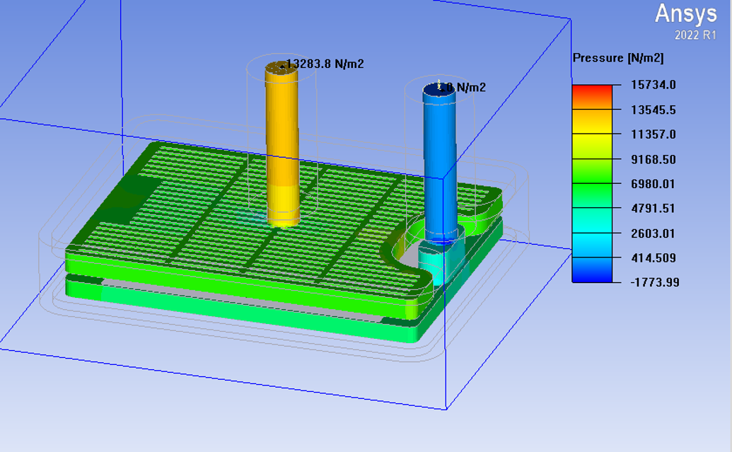
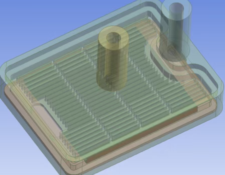
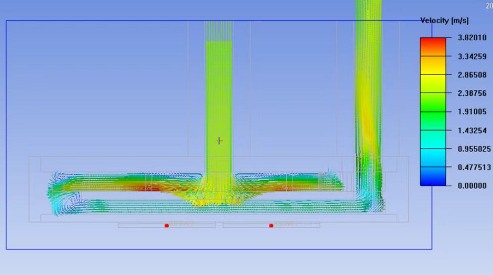
Targeting the 60×60mm standard chip heat source contact surface, the structure adopts an upper and lower double-layer stacked layout with independent and collaboratively operating coolant flow channels, achieving comprehensive performance upgrades compared with traditional single-layer planar structures. First, the three-dimensional layered stacking structure greatly increases the effective heat exchange area in a limited space, breaking the area limitation of planar structures and enabling bidirectional and hierarchical heat conduction for chip heat sources. Second, the layered structure effectively shortens the transmission path of heat from the chip core to the coolant, reducing heat conduction loss and thermal delay, which is highly consistent with the core logic of “reducing τ and minimizing loss” of Huawei Tau architecture. Third, the double-layer flow channels achieve double heat exchange flux, significantly improving coolant heat exchange efficiency, rapidly taking away concentrated heat from the chip and avoiding local heat accumulation and hot spot formation.
4. Homology Analysis Between Double-Layer Liquid Cooling Structure and Huawei Tau Architecture
The core breakthrough of Huawei Tau architecture is breaking the bottleneck of two-dimensional planar design. Through three-dimensional stacking and hierarchical layout of chip circuits, it shortens electrical signal transmission paths, reduces RC delay, and improves overall chip performance and energy efficiency without relying on advanced manufacturing processes.
The double-layer liquid cooling heat dissipation structure developed byKENFA TECH is highly consistent with this innovative concept, only converting the optimization object from “electrical signal transmission” to “heat energy transmission”. The two designs share identical core logic: both abandon inefficient traditional planar layouts and reconstruct energy transmission paths through three-dimensional hierarchical stacking. By shortening the transmission distance of energy (signals or heat), reducing transmission loss and improving space utilization, the system efficiency is significantly improved. Huawei Tau architecture solves the delay and loss problems of electrical signal transmission in chips, while the KENFA TECH double-layer stacked liquid cooling structure solves the thermal resistance and heat accumulation problems of heat transmission in high-power chips, realizing the effective implementation and extension of the three-dimensional hierarchical efficiency enhancement concept in the field of thermal management.
5. Application Advantages and Engineering Value of the Structure
Compared with traditional single-layer liquid cooling solutions, the double-layer stacked cooling plate structure of KENFA TECH has prominent advantages in high-power-density chip scenarios. In the 60×60mm heat source matching scenario, the structure effectively reduces the overall thermal resistance of the heat dissipation system, greatly improves heat dissipation efficiency, quickly balances the surface temperature of the chip, eliminates hot spot temperature differences, and prevents chip performance attenuation and frequency reduction caused by high temperature.
Relying on three-dimensional stacking efficiency enhancement, this structure does not require oversized heat dissipation space, featuring strong space adaptability and controllable comprehensive cost. This design verifies the universality of the Huawei Tau three-dimensional hierarchical concept, proving that the core idea of three-dimensional stacking and transmission path shortening is not only applicable to chip circuit design, but also can be widely extended to the thermal management of high-end electronic equipment. It provides a new lightweight and high-efficiency solution for heat dissipation optimization of high-power and high-heat-flux chips.
6. Conclusion
Aiming at the heat dissipation dilemma of high-power-density chips, KENFA TECH proposes and designs a double-layer stacked liquid cooling plate structure based on the three-dimensional hierarchical stacking core concept of Huawei Tau architecture, breaking the performance bottleneck of traditional planar heat dissipation schemes. Through three-dimensional hierarchical layout, the structure effectively expands the heat exchange area, shortens the heat transmission path, reduces heat dissipation loss, and significantly improves the heat dissipation efficiency and operational stability of chips under high-load conditions. This design realizes the cross-domain application of innovative chip architecture concepts in thermal management, providing a novel technical idea for heat dissipation optimization of high-end computing power chips and industrial high-power chips, with high engineering application value and technical innovation significance.
You can alos email to us king@kenfatech.com,we can share you more information about the designing.