
1. Introduction
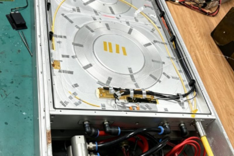
Thermal design for opticalmodules.With the rapid iteration of 800G and 1.6T high-speed optical interconnection systems, 224Gbps PAM4 has become the mainstream single-lane transmission standard for next-generation optical modules, silicon photonic chips, and thin-film lithium niobate modulators. Unlike traditional low-speed digital signals that are merely restricted by rise time and impedance matching, ultra-high-frequency signals above 56GHz exhibit prominent electromagnetic wave characteristics, including wavelength compression, dielectric-dependent propagation, resonant interference, and electromagnetic radiation leakage. These physical effects fundamentally determine the ultra-fine linewidth, ultra-narrow spacing, and high-precision layout rules of modern high-speed PCB and packaging substrates.
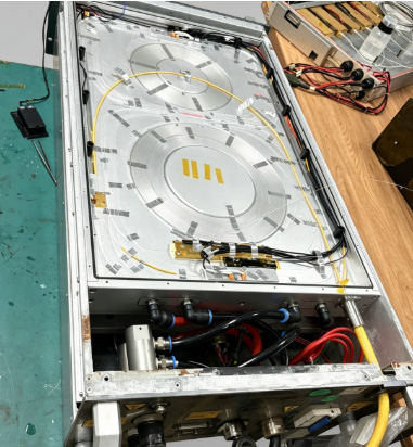
In parallel with electrical design optimization, the continuous improvement of signal bandwidth and integration density drastically increases power consumption and heat flux density of DSP chips, EML lasers, and high-speed driving circuits. Thermal-induced wavelength drift, dielectric constant variation, and impedance deviation will severely degrade high-frequency signal integrity. Therefore, thermal management solutions represented by heat sink air cooling and liquid cold plate liquid cooling are no longer independent heat dissipation designs but essential co-design links for high-frequency signal stability. This article systematically elaborates the physical essence of high-speed signal layout scaling, summarizes key high-frequency design pain points, and clarifies the collaborative mechanism between electrical refinement design and hierarchical thermal management.
2. Electromagnetic Wave Foundation: Frequency-Dominated Wavelength Compression in Dielectrics
All high-speed electrical signals and optical signals conform to the basic electromagnetic propagation formula λ = c/f, where wavelength is inversely proportional to signal frequency. As the signal rate rises to 224Gbps PAM4, the Nyquist fundamental frequency reaches 56GHz, and the actual operating bandwidth needs to be extended beyond 70GHz for engineering margin. Such ultra-high frequency sharply shortens the free-space wavelength, while the dielectric medium of PCB, packaging substrates, and photonic chips further compresses the propagation wavelength via refractive index modulation.
Different from vacuum propagation, the actual wavelength in dielectric materials is λ_eff = λ₀/√ε_r, where √ε_r is defined as the RF refractive index or compression coefficient. Higher dielectric constant brings more severe wavelength compression, making the electromagnetic wave more sensitive to structural dimensional changes. This is the core reason why high-frequency signals require extremely strict dimensional control of routing, electrodes, and packaging structures.
A typical physical feature of electromagnetic waves is the 1/4 wavelength resonant interference effect. Laser devices such as VCSEL, DFB, and EML actively adopt 1/4 wavelength grating resonant cavity superposition to amplify optical signals and enhance radiation efficiency. Conversely, high-speed electrical routing must completely avoid approaching the 1/4 wavelength size. Once the line spacing, line length, or dielectric thickness is close to the resonant dimension, electromagnetic waves will interfere and radiate outward, causing severe EMI interference and signal attenuation. The wavelength compression performance of mainstream optoelectronic materials is sorted in the table below.
3. High-Speed Anti-EMI Layout Principle: Spacing Scaling and Electromagnetic Coupling Termination
The design logic of high-speed electrical signals is completely opposite to that of antenna and laser devices. The core goal of high-density routing is tosuppress electromagnetic radiation and confine electromagnetic fields inside the transmission structure to avoid EMI leakage. Under ultra-short wavelength conditions, any inappropriate structural size will trigger resonance and radiation, so the industry has formed a unified design rule: all routing and electrode spacing must be controlled within 1/12 ~ 1/20 of the compressed dielectric wavelength to eliminate resonant margins.
To meet ultra-small wavelength dimensional constraints, high-speed layout requires synchronous reduction of three core parameters: signal line width, differential pair line spacing, and dielectric thickness between signal lines and GND reference plane. Reducing the dielectric thickness essentially shortens the return path of high-frequency current, strengthens the electric field and magnetic field coupling between the signal line and the ground plane, and realizes charge termination and field confinement. Compared with microstrip lines, stripline structures have fully symmetric dielectric layers, more uniform field distribution, and better anti-radiation performance, which are more suitable for 70GHz+ ultra-high-frequency scenarios.
With the upgrading from 112Gbps to 224Gbps PAM4, the engineering bandwidth margin and layout precision requirements are significantly improved. The following table summarizes the industry-standard layout spacing specifications for mainstream high-speed signal rates.
|
Signal Transmission Rate
|
Nyquist Frequency
|
Engineering Reserved Bandwidth
|
Layout Spacing Control Standard
|
Core Design Purpose
|
|---|---|---|---|---|
|
224Gbps PAM4
|
56GHz
|
≥70GHz
|
1/12 ~ 1/20 of compressed dielectric wavelength
|
Suppress high-frequency resonance, eliminate EMI radiation, ensure ultra-high bandwidth signal integrity
|
|
112Gbps PAM4
|
28GHz
|
≥35GHz
|
1/10 ~ 1/15 of compressed dielectric wavelength
|
Balance process difficulty and signal anti-interference capability
|
|
≤25Gbps NRZ
|
≤12.5GHz
|
Conventional margin
|
No strict wavelength proportional restriction
|
Meet basic impedance matching and transmission requirements
|
4. Multi-Dimensional High-Frequency Design Challenges and Systematic Optimization Solutions
Ultra-fine linewidth and narrow spacing layout are only the basic hardware conditions for high-speed signal transmission. High-frequency and short-wavelength operating conditions bring a series of derivative design challenges involving impedance continuity, dielectric uniformity, copper foil loss, and parasitic resonance. These factors will cause signal reflection, delay skew, scattering loss, and noise amplification, seriously reducing the system signal-to-noise ratio. This chapter systematically sorts out all key pain points and targeted optimization schemes.
|
High-Frequency Design Challenge
|
Physical Root Cause
|
Negative Influence on Signals
|
Engineering Optimization Solution
|
|---|---|---|---|
|
Impedance Discontinuity & Reflection Interference
|
Abrupt changes in line width, via size, and layer switching cause local impedance mutation
|
High-frequency electromagnetic reflection, noise superposition and amplification, reduced SNR
|
Implement full-path impedance simulation and calibration, unify via and routing specifications, eliminate impedance mutation points
|
|
PCB Glass Fiber Dielectric Inhomogeneity
|
Dielectric constant mismatch between glass fiber and resin leads to inconsistent wavelength compression
|
Differential signal delay skew, common-mode noise surge, failure of differential coupling
|
Adopt low-Df homogeneous high-speed dielectric materials, optimize fiber weaving direction and layout
|
|
High-Frequency Copper Foil Scattering Loss
|
Ultra-short high-frequency waves are extremely sensitive to copper foil roughness, causing severe scattering loss
|
Increased insertion loss, bandwidth attenuation, deteriorated eye diagram
|
Adopt ultra-smooth low-profile copper foil; optimize optical chip adhesive process to compensate for reduced bonding area
|
|
Via Stub & Annular Parasitic Resonance
|
Compressed short wavelength amplifies parasitic resonance effects of via stubs and GND hollow structures
|
Local electromagnetic resonance generates spurious noise, distorts high-speed signal waveform
|
Adopt stub-free via design, optimize GND plane integrity, avoid closed annular resonant structures
|
5. Thermal Co-Design for High-Frequency Optical Modules: Heatsink and Liquid Cold Plate Application
The ultra-fine and high-density electrical layout of 224G+ high-speed optical modules greatly improves signal transmission performance but also brings two prominent thermal problems: high heat flux density of core chips and poor internal heat dissipation channels. Long-term high-temperature operation will cause dielectric constant drift, wavelength shift, and impedance fluctuation, which indirectly destroy the high-frequency electromagnetic coupling state and lead to signal performance degradation. Therefore, hierarchical thermal management with heatsink air cooling and liquid cold plate liquid cooling is indispensable for stabilizing high-speed signal performance.
5.1 Heatsink Passive Air Cooling (Conventional Low-Medium Power Scenarios)
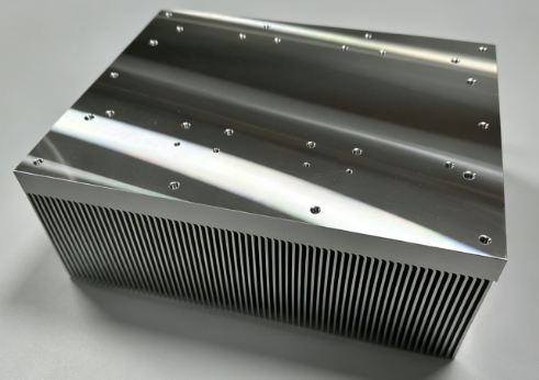
Heat sink is the most widely used passive heat dissipation structure for traditional optical modules. It relies on high-thermal-conductivity metal fins to expand the heat exchange area and takes away heat through natural convection or forced air cooling of the chassis. This solution has the advantages of simple structure, low cost, no power consumption, and high compatibility, which can fully meet the heat dissipation requirements of low-power 25G~112G optical modules.
However, in 224G ultra-high-frequency scenarios, the power consumption of DSP and EML devices increases exponentially, and passive heatsink cooling faces obvious bottlenecks. Limited by air heat transfer efficiency, it is impossible to eliminate local hotspots in a timely manner. Long-term high temperature will cause continuous drift of high-frequency signal parameters, increased bit error rate, and reduced system stability. Thus, heatsink can only be used as auxiliary heat dissipation for low-power high-speed modules.
5.2 Liquid Cold Plate Active Liquid Cooling (High-End 800G/1.6T Scenarios)
For ultra-high-speed, high-power optical modules above 224Gbps, liquid cold plate has become the standard thermal management solution for industrial high-end equipment.Different from passive air cooling, the liquid cold plate relies on internal micro-channel circulating coolant to realize efficient active heat exchange, with a heat dissipation efficiency more than 3 times that of traditional heatsink air cooling. It can quickly take away concentrated heat from DSP chips, laser chips, and driving circuits, realizing high-precision temperature control. At present, there are two mainstream liquid cold plate application forms in the industry. The first is cabinet-mounted fitting liquid cooling, which is compatible with existing QSFP-DD and OSFP packaging.
The liquid cold plate is fixed in the switch cage, and the module shell is closely attached to the cold plate to conduct heat, with low transformation cost and strong versatility. The second is module-embedded integrated liquid cooling, which directly integrates micro-channel cold plates inside the optical module, completely eliminating contact thermal resistance and achieving extreme heat dissipation, which is suitable for next-generation 1.6T ultra-high-density optical interconnection systems. The stable and low-temperature operating environment provided by the liquid cold plate can effectively suppress dielectric constant fluctuation and wavelength drift, maintain the optimal electromagnetic coupling state of fine-pitch routing, and fundamentally guarantee the long-term stability of high-frequency signal integrity. The detailed performance comparison of the two thermal management solutions is shown in the table below.
|
Thermal Solution
|
Heat Dissipation Mechanism
|
Relative Heat Exchange Efficiency
|
Temperature Control Accuracy
|
Applicable Product Grade
|
Advantages & Limitations
|
|---|---|---|---|---|---|
|
Heatsink Air Cooling
|
Passive convection heat dissipation via metal fin expansion area
|
1.0 (Benchmark)
|
Low, susceptible to ambient temperature
|
25G~112G Low-power optical modules
|
Cost-effective and maintenance-free, but unable to solve high heat flux hotspots, not suitable for 70GHz+ high-frequency scenarios
|
|
Liquid Cold Plate Liquid Cooling
|
Active circulating heat exchange through internal micro-channel coolant
|
≥3.0 times of air cooling
|
High, precise constant temperature control
|
224G/800G/1.6T High-speed high-power modules
|
Thoroughly eliminate hotspots, stabilize high-frequency signal parameters; slightly higher cost and requires supporting liquid circulation system
|
6. Conclusion: Electrical-Thermal Co-Design Core Philosophy for High-Speed Optical Modules