
Abstract
For decades,microchannel cooling technology ,the development of the semiconductor industry has been driven by process scaling, which continuously shrinks transistors to improve chip computing power. However, as semiconductor manufacturing processes approach physical limits, concentrated challenges such as quantum leakage, surging process complexity, and runaway manufacturing costs have rendered the traditional Moore’s Law iteration path unsustainable. Proposed by Huawei, the Tau (τ) Law breaks away from the inherent reliance on advanced manufacturing processes. Instead, it adopts a “time-for-performance” approach by optimizing circuit time constants, restructuring logical architectures, and implementing 3D heterogeneous stacking, enabling mature processes to deliver computing performance comparable to advanced nodes. While the industry focuses heavily on its architectural innovation and performance improvement, few discussions have thoroughly explored the thermal changes brought by this new architecture. The Tau Law not only reshapes the iteration logic of chip computing power but also subverts the traditional thermal management system that has been applied for decades. Transient thermal shocks caused by time folding and confined heat accumulation resulting from 3D stacking form unprecedented thermal challenges that cannot be solved by conventional heat dissipation solutions. Based on practical engineering logic of chip thermal management, this paper thoroughly analyzes the thermal pain points under the Tau Law architecture, sorts out Huawei’s comprehensive heat dissipation solutions covering chip core, interlayer packaging, and system levels, and clarifies the new industry rule that “thermal management capability defines the upper limit of chip computing power” in the post-Moore era.
1. Introduction: Computing Power Transformation — Traditional Thermal Management Systems Fail to Keep Pace
For a long time, process precision has served as the core criterion for evaluating chip performance and semiconductor progress. The industry’s underlying logic is straightforward: densifying and miniaturizing transistors spatially improves computing power and optimizes power consumption. Under the Moore’s Law iteration model, chips feature stable thermal characteristics, uniform heat distribution, and gentle temperature rise, belonging to typical steady-state planar heat dissipation scenarios. Mainstream cooling solutions such as air cooling, vapor chambers, and conventional liquid cooling are all designed to adapt to such planar, steady-state, and uniform thermal conditions, fully meeting the heat dissipation requirements of traditional chips.
In recent years, however, the industry landscape has undergone fundamental changes. The R&D and construction costs of advanced process fabs have soared to tens of billions. Quantum tunneling effects at the atomic scale are inevitable, and advanced processes suffer from higher leakage power consumption and lower yield rates, completely exhausting the performance gains from dimensional scaling. Meanwhile, scenarios including AI large model training, autonomous driving, and cloud supercomputing continue to drive explosive growth in computing demand, making traditional paths incapable of matching industrial development. Against this backdrop, Huawei’s Tau (τ) Law emerges as a brand-new iteration path for the semiconductor industry.
Different from conventional architectural fine-tuning, the Tau Law represents a fundamental industrial transformation. While Moore’s Law pursues performance through spatial scaling, the Tau Law improves performance by compressing the circuit time constant (τ). It greatly reduces transistor switching delay and data transmission latency via logical circuit rearrangement, signal path optimization, and 3D stacked interconnection. In short, instead of pursuing continuous device miniaturization, it accelerates chip operation and enhances efficiency through architectural optimization, enabling chips built on mature processes to deliver performance equivalent to advanced process nodes.
Nevertheless, this innovative transformation brings critical engineering challenges, foremost being the complete failure of traditional thermal management systems. Conventional heat dissipation targets slow, stable, and planar heat generation, whereas chips based on the Tau Law adopt high-speed time-dimensional operation combined with high-density 3D spatial integration, leading to a completely overhauled heat generation mechanism. It is fair to state that thermal management is no longer an auxiliary feature but the core bottleneck restricting the mass production and stable operation of Tau Law technologies.
2. In-Depth Analysis of Thermal Pain Points Under the Tau Law Architecture
Most public interpretations simply attribute thermal challenges to “more stacking layers and higher heat generation”, which only scratches the surface. The fundamental unsolvable thermal dilemma stems from the superposition of transient thermal shocks caused by time folding and thermal resistance barriers formed by 3D confined stacking, creating a dead end for traditional heat dissipation technologies.
2.1 Time Folding: Failure of Steady-State Heat Dissipation and Hidden Dangers of Extreme Transient Thermal Shocks
Traditional chips operate with stable loads and minor power fluctuations, releasing heat continuously and steadily and allowing sufficient time for heat conduction and dissipation. In contrast, the Tau Law compresses time constants to maximize logical unit switching frequency and data throughput, fundamentally altering chip operating characteristics.
The most intuitive difference lies in heat generation patterns: traditional chips produce uniform and continuous heat, while Tau Law-based chips generate high-frequency pulsed heat. During instantaneous high-load scenarios such as large model inference and high-density computing, the chip produces ultra-high power consumption and intense transient heat flux within microseconds. The temperature rises sharply in an instant, and traditional heat dissipation structures suffer from inherent response lag, failing to cool down timely. Before heat dissipation systems fully activate, core temperatures exceed safety thresholds, causing frequency reduction, computing power drop, and logical operation errors. Long-term operation further accelerates device aging and shortens service life, representing an unprecedented thermal challenge for traditional planar steady-state chips.
2.2 3D Stacking: Confined Interlayer Structure Forming Insurmountable Thermal Resistance Barriers
To match the ultra-high computing power brought by time folding, the Tau Law adopts high-density 3D heterogeneous stacking architecture, which vertically integrates computing, storage, interconnection, and power supply chips. Traditional planar chips expose all heat-generating surfaces to the external environment, enabling unobstructed heat conduction and dissipation.
In contrast, the multi-layer sandwich structure of 3D stacking encapsulates core heat-generating units between layers, triggering two fatal problems. First, thermal resistance accumulates layer by layer. Stacked silicon wafers, dielectric layers, and interconnection layers significantly extend the heat conduction path from the core to external heat sinks, leading to a geometric increase in overall thermal resistance. Second, dead-space heat accumulation occurs in interlayer gaps. The micron-scale interlayer spacing eliminates air convection, resulting in persistent high-temperature hotspots caused by undissipated heat.
More importantly, Tau Law stacking is not simple physical superposition but in-depth functional integration. All layers participate in high-frequency computing without low-temperature auxiliary or idle heat dissipation layers, operating under simultaneous high heat consumption. This drastically amplifies thermal pressure compared with traditional stacked chips and exacerbates heat accumulation.
2.3 Multi-Physics Coupling: Mutual Restriction of Heat Dissipation, Computing Performance and Reliability
Under the ultra-compact and highly integrated architecture, chip internal space is fully occupied by signal lines, power channels, and logical units. Adopting traditional external heat sinks or thick thermal conductive structures will inevitably occupy valid computing space and offset the performance gains brought by time folding.
Meanwhile, frequent instantaneous temperature fluctuations cause continuous thermal expansion and contraction of materials, easily triggering interlayer solder joint detachment, dielectric layer cracking, and interconnection failure. This forms the most intractable triangular engineering contradiction: extreme computing power requires high-density integration, high-density integration leads to severe heat accumulation, and excessive heat dissipation structures sacrifice performance and reliability. This is the core reason why the Tau Law requires a fundamental restructuring of thermal management solutions.
3. Huawei’s Full-Stack Thermal Management Solution: Engineering Practices Adapted to the Tau Law
Facing these unprecedented thermal challenges, Huawei abandons the industry’s conventional “chip-first, heat-dissipation-later” model and adopts integrated co-design of chips, architecture and thermal management. During the initial stage of logical folding and 3D stacking layout, heat conduction paths and cooling structures are pre-planned. A complete thermal system covering core, interlayer, packaging, and system levels is established to solve the industry pain points of poor adaptability and low yield of thermal solutions for high-computing dense architectures.
3.1 Chip Core Level: Fixed-Point Embedded Diamond Structure for Transient Heat Accumulation Suppression
Targeting pulsed transient high heat caused by time folding, Huawei abandons traditional full-coverage thermal solutions and adopts micro-region fixed-point heat dissipation optimized for actual operating conditions. Chip heat generation is non-uniform, with most heat concentrated in core computing units and high-frequency switching circuits.
Based on this feature, Huawei etches micron-scale grooves in hotspot areas during chip manufacturing and embeds high-purity diamond thermal units. Diamond exhibits far higher thermal conductivity than copper and aluminum with excellent insulation, avoiding interference with signal transmission and logical operation. Its core advantage lies in ultra-fast transient thermal response, which captures instantaneous peak heat within microseconds and eliminates temperature spikes, solving the response lag of traditional cooling technologies. Meanwhile, the lightweight embedded structure occupies negligible computing space and fully preserves the performance gains of time folding.
3.2 Stacking Interlayer Level: Vertical Thermal Columns + Microfluidic Cooling to Break Confined Thermal Barriers
Interlayer heat accumulation is the biggest pain point of 3D stacking. Huawei adopts a dual collaborative solution combining passive heat conduction and active liquid cooling to completely eliminate confined thermal resistance issues.
In terms of passive heat conduction, the industry’s conventional planar TIM thermal gaskets are replaced with vertical diamond thermal column arrays implanted between stacking layers. These thermal columns penetrate dielectric and functional layers, building straight high-speed vertical heat conduction channels to export internal accumulated heat efficiently. In addition, diamond has a thermal expansion coefficient highly consistent with silicon, preventing cracking and delamination under repeated temperature cycling and ensuring long-term operational stability.
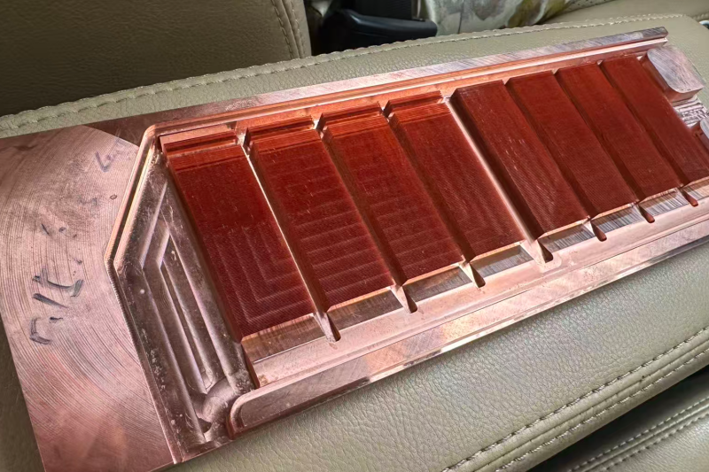
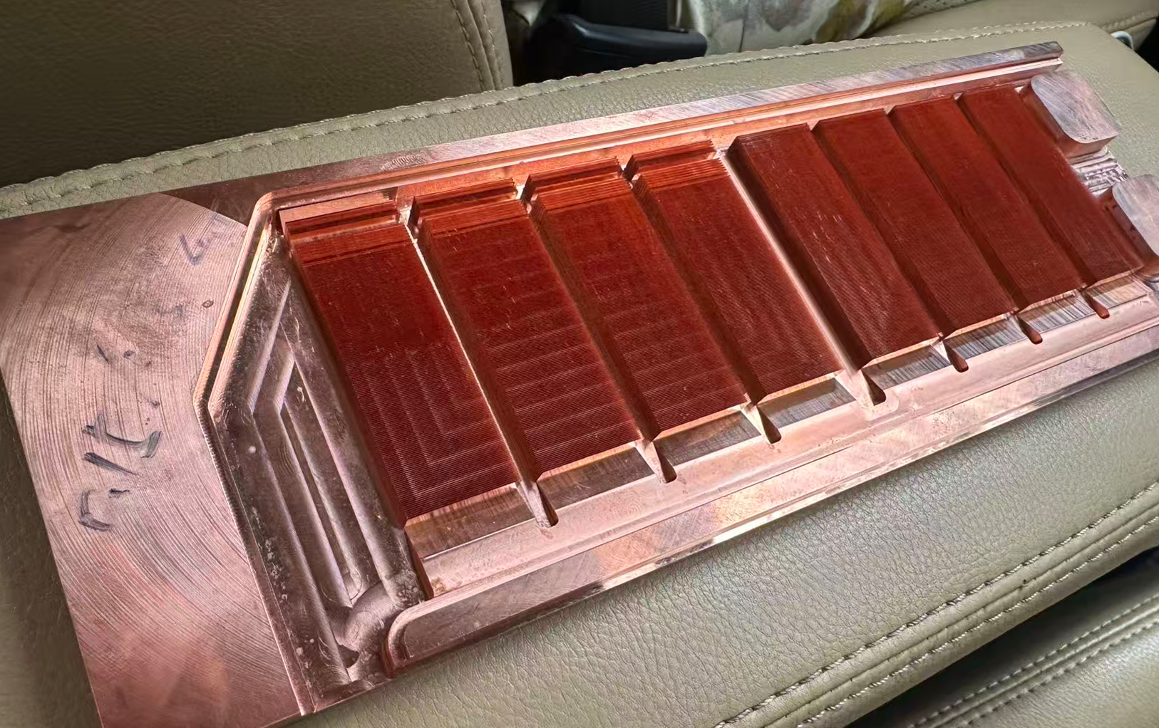
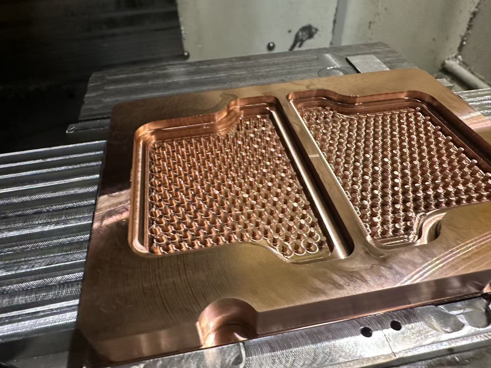
In terms of active heat dissipation, Huawei integrates KENFA self-developed Skived Fin microchannel structure embedded microfluidic cooling solution in the tiny gaps of stacked interlayers, revolutionizing the heat exchange efficiency of traditional liquid cooling. As KENFA’s core thermal management technology, the proprietary Skived Fin skiving process requires no welding and generates zero interfacial thermal resistance. The integrally molded micron-scale dense skived fins and microchannel arrays greatly expand the effective heat exchange area between coolant and the thermal substrate. Featuring high channel precision and uniform flow resistance, it perfectly adapts to the micron-level narrow space of chip interlayers. Different from traditional external water cooling and ordinary stamped microchannels, this in-situ cooling structure instantly carries away heat during generation, completely eliminating interlayer dead-space heat accumulation. It stably withstands the ultra-high transient heat flux of Tau Law architectures and fully meets the extreme heat dissipation demands of high-load computing scenarios.
3.3 Packaging Level: Gradient Composite Substrate for Full-Link Thermal Resistance Matching
Most chip thermal failures originate from thermal blocking at packaging interfaces rather than core heat accumulation. To address this engineering pain point, Huawei develops self-designed gradient copper-diamond composite packaging substrates. Unlike single-ratio composite substrates on the market, this product adopts a layered gradient structure: the inner layer is densely arranged with diamond to maximize thermal conductivity and rapidly export core heat, while the outer layer adopts high-toughness metal materials to ensure structural strength and welding reliability.
This structure perfectly matches the “core ultra-high heat, outer uniform temperature” thermal characteristics of Tau Law chips, significantly reducing packaging interfacial thermal resistance. It forms a complete and uninterrupted heat conduction link from core thermal columns to system cold plates, avoiding heat accumulation at the packaging layer and achieving zero weak links in full-link heat dissipation.
3.4 System Level: Intelligent Dynamic Thermal Management Adapted to Fluctuating Computing Loads
Tau Law chips deliver unfixed computing power, with drastically different power consumption and heat generation under no-load, light-load, and full-load conditions. Traditional fixed-power cooling systems either provide insufficient heat dissipation or cause excessive energy waste. Huawei builds a targeted intelligent dynamic thermal management system that monitors chip computing load, time constants and transient temperatures in real time, and dynamically adjusts microfluidic flow rate, cooling temperature and overall heat dissipation power.
Combined with the KENFA Skived Fin microchannel liquid cooling assembly and full-domain immersion cooling solution, it leverages the zero-interfacial-thermal-resistance advantage of integral skiving structures to maintain high-efficiency heat exchange and eliminate system-level thermal dead zones. This ensures stable chip temperatures during long-duration high-frequency operation and full-load computing, completely solving the industry-wide problem of “higher performance accompanied by runaway heat generation” for high-end high-computing chips.
4. Core Innovative Value: Redefining the Rules of Computing Power and Heat Dissipation in the Post-Moore Era
Essentially, Huawei’s thermal management system represents a fundamental restructuring of industrial thermal logic, rather than a simple technical upgrade. Traditionally, heat dissipation was a secondary auxiliary component of chip design, which could be optimized retroactively after performance validation. The Tau Law completely reverses this logic.
In the post-Moore era, the upper limit of computing power for mature processes is no longer determined by process precision, but by thermal management capability. The ability to solve transient ultra-high heat flux and interlayer heat accumulation enables continuous computing power improvement through architectural stacking and time compression, constituting the core competitiveness of the Tau Law. While most industrial stacking cooling solutions only passively solve heat problems caused by physical superposition, Huawei’s thermal system is uniquely designed for the new “time-for-performance” architecture, resolving fundamental engineering contradictions of paradigm iteration with strong forward-looking advantages.
Supported by Huawei’s architectural innovation and full-link thermal management mass-production capabilities, this technical system not only guarantees the large-scale deployment of Huawei’s high-end chips but also provides a feasible and mass-producible architectural innovation and thermal management solution for the global post-Moore semiconductor industry.
5. Conclusion and Industry Outlook
The spatial scaling path of Moore’s Law has reached its physical end, and the semiconductor industry has entered a new stage driven by architectural innovation. Breaking free from process involution, Huawei’s Tau (τ) Law achieves hardware limit breakthroughs through time-dimensional optimization, providing a revolutionary development path for the global semiconductor industry. The stable implementation of this innovative system is strongly supported by Huawei’s original architecture and full-link thermal management technology with excellent adaptability and engineering practicability.
Future AI computing, general-purpose computing and high-performance chips will inevitably develop toward high-density stacking and high-dynamic operation, making transient ultra-high heat flux and multi-physics coupled heat accumulation common challenges for all high-end chips. Thermal management will upgrade from auxiliary support to the core barrier restricting computing power iteration.KENFA’s core Skived Fin microchannel thermal management technology, with its unique advantages of zero interfacial thermal resistance, ultra-high heat exchange efficiency and excellent adaptability to miniaturized integrated scenarios, will become a key pillar for the large-scale implementation of high-computing chip thermal solutions in the post-Moore era.
Overall, the success of the Tau Law marks a dual breakthrough in architectural innovation and underlying engineering technology. Amid the global bottleneck of semiconductor process competition, Chinese enterprises have broken inherent industrial rules through original architecture and independent thermal management systems, providing a valuable Chinese solution for industrial upgrading in the post-Moore era.