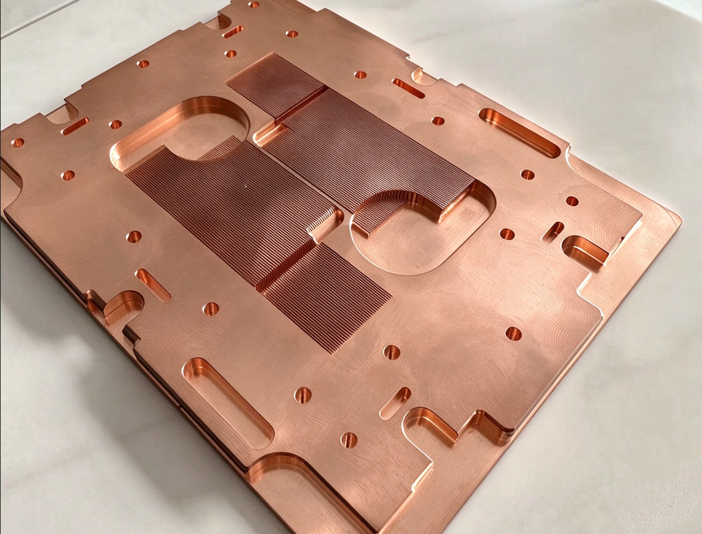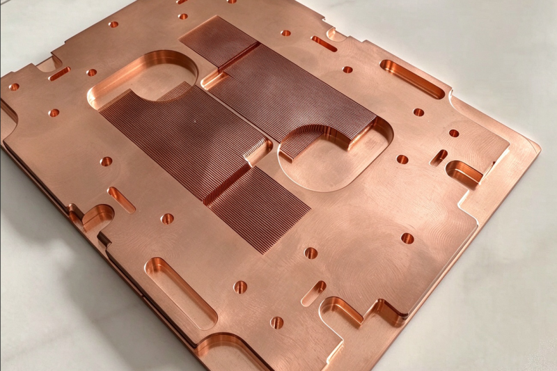
What It Is a diamond cold plate?
A diamond cold plate is a liquid cooling component fabricated with synthetic diamond or diamond composite as the core thermal conductive substrate, integrated with microchannels and manifold sealing structures. Unlike conventional aluminum or copper cold plates, it leverages diamond’s ultra-high intrinsic thermal conductivity together with convective heat transfer from circulating coolant to rapidly extract heat from high-power components such as chips, laser pump sources and optical modules.
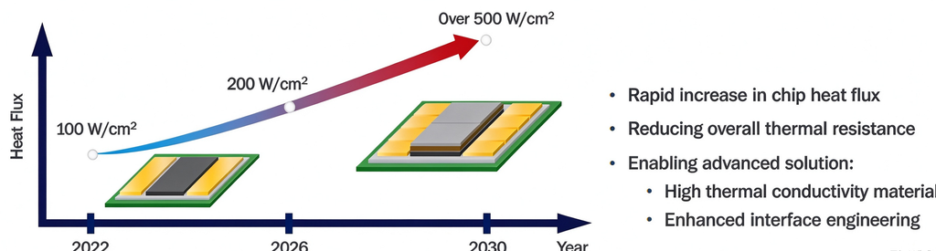
Diamond is emerging as a critical high-end thermal management material, driven by the fast expansion of high-power GPUs, advanced packaging and computing infrastructure. Continuous technological innovation runs through the whole industrial chain, from diamond processing and diamond-copper composite fabrication to deployment on high-power devices. Chip heat flux stood at roughly 100 W/cm² in 2022, reached around 200 W/cm² in 2026, and is projected to exceed 500 W/cm² by 2030. As heat flux rises sharply, overall thermal resistance must be reduced. The viable path combines high thermal conductivity materials with advanced interface engineering.
The simulation case discussed below uses a 3 kW heat source with a footprint of 32.2 × 25.7 mm². The calculated average heat flux is approximately 360 W/cm², which surpasses the 2026 baseline and aligns with the 2030 performance roadmap. This simulation validates the cooling requirements for next-generation chips. The fundamental thermal relationship follows: Q × Rth = ΔT. Taking a thermal resistance of 0.005 ℃/W as an example, 2000 W creates a 10 ℃ temperature rise, while 4000 W doubles the rise to 20 ℃. Higher power levels demand lower thermal resistance.
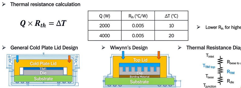
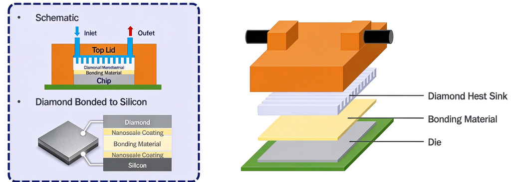
Wiwynn compared two structural schemes. The traditional cold plate stack is “lid + TIM1 + die”, where heat passes through thermal interface material before reaching the lid. The improved design bonds the microstructured lid directly onto the chip via bonding material and removes the separate lid and TIM1 layer. The thermal resistance chain is simplified from the chip junction (T_junction) to the coolant inlet (T_inlet): die thermal resistance R_die, interface thermal resistance R_TIM, and base-to-fluid thermal resistance R_base to ambient. From a material perspective, optimization is not limited to the cold plate substrate itself; the position and quantity of interface layers also become key tuning variables. This forms the core technical foundation of this article.
2,Why Diamond Cold Plates
Three mainstream material options are available: monolithic sintered diamond, diamond‑copper composite, and diamond‑SiC composite. Supported channel types include microchannels, manifold channels and serpentine channels, compatible with water cooling and fluorinated coolants. We recommend a diagonally symmetric inlet and outlet layout for balanced flow distribution and better cooling efficiency. We can revert to your original inlet/outlet layout per request, though the original configuration tends to form local hotspots and delivers lower heat transfer efficiency.
Chip heat flux keeps climbing: 100 W/cm² in 2022, 200 W/cm² in 2026, and forecasted above 500 W/cm² by 2030. Rising heat flux requires lower system thermal resistance, achieved by high‑conductivity substrates and robust interface engineering.
Material property benchmarks:
- Diamond: thermal conductivity > 2000 W/m·K, CTE ~1.0 ppm/K, density ~3.5 g/cm³, Young’s modulus 1050–1200 GPa
- Diamond‑copper composite: thermal conductivity 600–900 W/m·K, CTE 6.0–9.0 ppm/K, density 5.0–6.0 g/cm³
- Diamond‑SiC composite: thermal conductivity 500–800 W/m·K, CTE only 2.0–4.5 ppm/K, density 3.30–3.45 g/cm³
- Copper (reference): thermal conductivity ~400 W/m·K, CTE ~17 ppm/K, density 8.96 g/cm³
Three key observations:
- Diamond‑SiC has a CTE nearly matching silicon (2.6–3.3 ppm/K). It is ideal for positions close to the chip and roughly 60% lighter than copper, bringing benefits for rack weight control.
- Diamond‑copper offers superior thermal conductivity, yet its CTE sits between pure diamond and copper. Structural design is required to mitigate thermal stress.
- Diamond stiffness is 8–10 times that of copper. Stress from clamping force and thermal cycling carries higher failure risks.
The report draws an accurate conclusion: diamond delivers ultra-high thermal conductivity, while its low CTE creates integration and reliability challenges. Composites strike a balance between thermal performance and compatibility.
Two fundamental barriers hinder diamond adoption: - CTE mismatch: Diamond (~1.1 ppm/K), silicon (2.6–3.3 ppm/K) and copper (16–17 ppm/K) show large divergence. Thermal cycling accumulates stress at interfaces and causes cracking or delamination.
- Chemical inertness: Diamond cannot be directly joined to silicon or copper with standard assembly processes. Surface metallization is mandatory for reliable bonding.
This explains why diamond has long been known for excellent thermal conductivity yet remains limited in mass‑produced cold plates. Its thermal performance is sufficient; the real difficulty lies in long‑term stable bonding with surrounding silicon, copper and solder materials.
Three mainstream integration routes are widely studied: - Metallization + solder bonding: Compatible with existing packaging workflows for diamond‑copper or diamond‑silicon assembly. Performance depends heavily on metallization quality, solder wettability and interface stability. Suitable for thermal spreaders and package‑level thermal integration.
- Brazed joining: High mechanical strength and robustness. However, high‑temperature brazing introduces residual stress and risks interface damage, making it suitable for high‑reliability thermal modules.
The report states that thermal performance, reliability, manufacturability and cost must be traded off. Importantly, interface quality usually exerts a larger impact than the intrinsic thermal conductivity of diamond. A rough calculation illustrates this point (for reference only): a 1 mm thick diamond substrate over the 32.2 × 25.7 mm² area has a conductive thermal resistance of approximately 0.0006 ℃/W, while copper of the same thickness reaches 0.003 ℃/W. A 20 μm solder layer with thermal conductivity of 50 W/m·K yields a thermal resistance of 0.0005 ℃/W, comparable to the diamond substrate itself. The inherent advantage of high‑conductivity material can easily be erased by a poorly engineered interface.
Limitations of conventional metal thermal solutions: - Copper cold plate: ~400 W/m·K, density 8.96 g/cm³, CTE 17 ppm/K. Heavy weight and high CTE create significant mismatch with silicon chips. Thermal cycling leads to high interface stress, delamination and cracking.
- Aluminum cold plate: thermal conductivity capped at 200–230 W/m·K, high thermal resistance, unable to support ultra‑high heat flux.
- Ceramic substrate: limited thermal conductivity, brittle, difficult to machine into high‑aspect‑ratio microchannels.
3. How We Manufacture & Validate
Material Preparation,Diamond powder is blended with copper or SiC powder. Composite preforms are produced via vacuum hot pressing or melt infiltration. Diamond volume fraction typically ranges from 55 vol% to 70 vol% to balance thermal conductivity, machinability and CTE.
Channel Machining cold plate,CNC milling or laser ablation forms high‑aspect‑ratio microchannels. The simulated fin geometry follows these dimensions: fin width 0.1 mm, fin height 2 mm, base thickness 1 mm, a typical high‑aspect‑ratio microchannel design. Heat travels upward through slender fins, so fin material conductivity directly governs fin efficiency. The base performs lateral heat spreading. Therefore, the comparison evaluates separate material changes for fins and base. Split structures are sealed by vacuum brazing or active brazing.
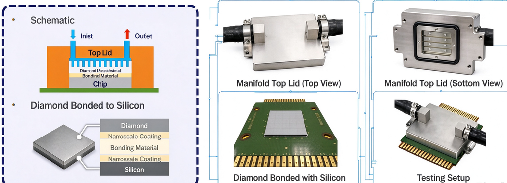
Interface Metallization and Bonding.The diamond‑silicon bonding stack adopts a five‑layer architecture: diamond → nano‑coating → bonding material → nano‑coating → silicon. The nano‑coatings serve as the metallization layer to overcome diamond inertness.
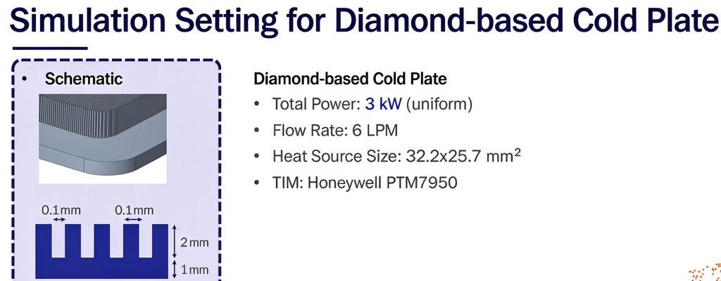
Simulation conditions:
3 kW uniform heat load, flow rate 6 LPM, heat source size 32.2 × 25.7 mm², TIM material Honeywell PTM7950.
Five material combinations were evaluated:
- All‑copper: maximum case temperature 106.83 ℃, cold plate base temperature 64.83 ℃, case‑to‑inlet thermal resistance 0.0256 ℃/W, base‑to‑inlet thermal resistance 0.0116 ℃/W
- Diamond‑copper base only: maximum case temperature 102.69 ℃, temperature reduction ~4.1 ℃
- Diamond‑copper base + fins: maximum case temperature 98.86 ℃, cumulative reduction ~8.0 ℃
- Full diamond base + fins: maximum case temperature 91.22 ℃, 15.6 ℃ lower than all‑copper; case‑to‑inlet thermal resistance reduced by 20% to 0.0204 ℃/W; base‑to‑inlet thermal resistance reduced by 46% to 0.0063 ℃/W
- Diamond‑SiC: results close to diamond‑copper (98.89 ℃ vs 98.86 ℃; thermal resistance 0.0230 ℃/W and 0.0089 ℃/W). This similarity comes from assigned simulation parameters and does not imply equivalent performance.
Two additional derived observations from the dataset:
- The temperature difference between case and cold plate base remains stable at ~42 ℃, corresponding to thermal resistance ~0.014 ℃/W, independent of cold plate material. For the full diamond design, this segment accounts for roughly 69% of total case‑to‑inlet resistance, compared with 55% for all‑copper. Once the substrate is upgraded, the thermal bottleneck shifts toward TIM and bonding interfaces.
- Coolant sensible heat rise contributes substantially to the remaining 0.0063 ℃/W of base‑to‑inlet resistance. Using water as coolant, 3 kW heat removed at 6 LPM creates a ~7 ℃ temperature rise, equivalent to 0.0024 ℃/W. Further performance gains are constrained by flow rate and convection, not solid conduction.
Beyond simulation, physical test benches are under construction. In this structure, diamond microchannels sit directly above the chip with bonding material in between. A manifold top cover with inlet and outlet ports sits on top. Coolant flows in, exchanges heat through microchannels, and exits. Manifold covers, diamond‑silicon bonded samples and full test fixtures have been fabricated, marking progress from simulation to hardware validation.
Outstanding issues remain: interface engineering is the primary bottleneck; thermo‑mechanical reliability needs verification under scaled conditions; manufacturability and yield require improvement. The team plans to complete thermal testing in September and has published the whitepaper Advanced Microchannel Materials — Diamond Composite Thermal Solutions. Wiwynn states in the whitepaper that diamond composite thermal conductivity reaches approximately 2000 W/m·K, targeting extreme local heat flux above 500 W/cm². The report closes with open discussion; measured data is pending release. Based on public information, simulation has proven diamond’s material advantage. Interface reliability, mechanical performance and cost are the three gates determining mass production readiness.
Surtec‑650 passivation is optional for corrosion resistance. Finished parts undergo pressure hold leak test, flow resistance test and thermal resistance calibration to confirm zero leakage and qualified heat transfer performance.
Limitations: Monolithic diamond blanks are extremely hard, with much higher machining cost than copper or aluminum. Large‑size and complex deep‑channel machining is difficult. Diamond cold plates fit high‑value low‑volume samples, demo kits and premium prototypes, not low‑cost consumer‑grade mass production.
4,Performance Comparison
| Item | Monolithic Diamond | Diamond‑Copper Composite | Diamond‑SiC Composite | Copper Cold Plate | 6063 Aluminum Cold Plate |
|---|---|---|---|---|---|
| Thermal Conductivity | >2000 W/m·K | 600–900 W/m·K | 500–800 W/m·K | ~400 W/m·K | ~200 W/m·K |
| CTE | ~1.0 ppm/K | 6.0–9.0 ppm/K | 2.0–4.5 ppm/K (silicon‑matched) | 17 ppm/K | 23 ppm/K |
| Density | 3.5 g/cm³ | 5.0–6.0 g/cm³ | 3.30–3.45 g/cm³ | 8.96 g/cm³ | 2.7 g/cm³ |
| Young’s Modulus | 1050–1200 GPa | — | — | — | — |
| Machining Difficulty | Extremely High | High | High | Medium | Low |
| Thermal Cycling Interface Risk | High (CTE mismatch with silicon) | Medium | Lowest | Moderately High | High |
| Applicable Heat Flux | >800 W/cm² | 500–800 W/cm² | 500–800 W/cm² | <600 W/cm² | <300 W/cm² |
| Cost | Extremely High | High | High | Medium | Low |
✅ Core conclusion: Diamond is not a universal upgrade. It is only justified when copper and aluminum solutions hit thermal limits and low thermal resistance, low thermal stress and long‑term reliability are mandatory requirements. Diamond composite solutions represent a trade‑off between thermal performance, reliability, manufacturability and cost.
5,Application Scenarios
1, GPU,High‑power semiconductor lasers and laser pump source cooling (primary focus)
2. CPO / NPO optical modules and high‑speed optoelectronic assemblies
3. Next‑generation AI chips, test prototypes and MCP demo kits for extreme heat flux >500 W/cm²
4. Aerospace radar and meteorological RF high‑power devices
5. Premium thermal bases paired with TEC cooling modules
6. Laboratory reliability test samples and customer demo kits (low volume, high specification)
6. FAQ
Q1: Can diamond cold plates adopt the same channel layout as regular copper cold plates?
A: Yes. Channel geometry and inlet/outlet positions are fully customizable. We recommend diagonally symmetric inlet and outlet for uniform flow and better cooling efficiency. We can revert to your original layout upon request, though this layout tends to create hotspots and reduce heat transfer efficiency.
Q2: Can diamond bond directly to chips?
A: Bare diamond is chemically inert and cannot be brazed directly. Nano‑metallization coating is required first. We provide titanium / nickel metallization processes to enable reliable bonding with solder and substrates, compatible with the five‑layer bonding stack.
Q3: Where is the real thermal bottleneck for diamond solutions?
A: Once substrate conductivity reaches a high level, the bottleneck shifts from solid conduction to interfaces (TIM and bonding layers) and coolant convection. Even premium diamond substrates lose their advantage if interfaces are poorly engineered. Coolant temperature rise also creates a physical ceiling; switching to higher‑conductivity solids delivers minimal gain once convection saturates.
Q4: Can diamond cold plates be mass produced?
A: Current offerings target engineering samples, test units and low‑volume high‑end orders. Mass production is constrained by raw material cost, metallization maturity and yield. As stated in Wiwynn’s whitepaper, interfaces, reliability and cost are the three major barriers for scaling. We also evaluate cost‑effective copper microchannel alternatives once customer testing completes and projects ramp up.
Q5: What coolant media are compatible?
A: Deionized water, ethylene glycol mixtures and fluorinated coolants are all supported, same as standard liquid cooling systems. Corrosion protection is implemented alongside sealing structures.
7,What can help you from Kenfa Tech
Kenfa tech provides custom diamond composite cold plate and heat sinks development services, including thermal simulation evaluation, drawing design, sample fabrication, metallization bonding, leak inspection and thermal resistance testing. We assess monolithic diamond, diamond‑copper, diamond‑SiC or copper‑aluminum microchannel options based on your heat flux, footprint and CTE matching targets, and help mitigate interface stress and thermal bottleneck risks.Submit your component specifications and drawings for technical review and quotation king@kenfatech.com.