
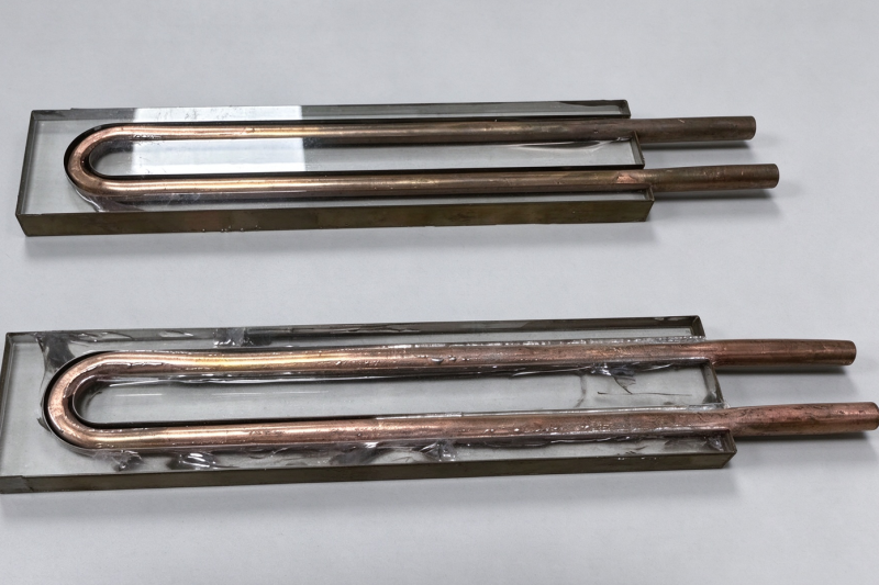
This article introduces the glass‑substrate cold plate with embedded copper tubes developed by KENFA TECH for high‑speed, high‑power optical modules. We are jointly researching this solution with SCHOTT, a world‑leading glass manufacturer. Using this specialty glass, we fabricate this cold plate and integrate it into the optimal thermal coupling position inside optical modules. Derived from the mature aluminum plate design with embedded copper tubes, this solution replaces the substrate with this specialty glass to fundamentally mitigate optical drift and galvanic corrosion caused by metal cold plates. Below we discuss material characteristics, working principles, process challenges, simulation pitfalls and selection criteria to support thermal design evaluation in the early R&D stage of liquid cooling plate for optical modules.
1. Two Hidden Limitations of Metal Cold Plates for High‑Power Optical Modules: Optical Drift and Galvanic Corrosion
For 800G, 1.6T and next‑generation 3.2T high‑power CPO and silicon photonic modules, heat dissipation demand keeps rising, resulting in larger temperature swings. Aluminum or copper cold plates with embedded copper tubes are widely adopted due to mature thermal manufacturing and good thermal performance. However, two inherent drawbacks are hard to eliminate by structural optimization: thermally induced optical drift and galvanic corrosion between dissimilar metals.
- Mechanism of thermally induced optical drift Silicon photonic chips, optical waveguides and glass bridges feature ultra‑low coefficient of thermal expansion (CTE). In contrast, copper and aluminum are high‑CTE metals. Under power cycling and temperature cycling, metal cold plates expand and contract visibly. Deformation transfers through TIM layers to optical chips and coupling interfaces, causing relative displacement between fiber arrays, grating couplers and silicon waveguides. Optical coupling is extremely sensitive to micron‑scale movement. Tiny displacement leads to increased insertion loss, wavelength shift and unstable bit error rate. Higher power brings larger temperature rise and greater deformation. Simply improving cooling capacity and lowering junction temperature can reduce temperature rise, yet cannot resolve the fundamental CTE mismatch between metals and optical components.
- Mechanism of galvanic corrosion Tiny moisture, flux residues, condensed water and ionic contaminants may exist inside optical module packages. Copper, aluminum, nickel plating, silicon photonic electrodes and solder are metals with different electrochemical potentials. When they contact each other in the presence of ion‑containing conductive media, a galvanic cell forms and triggers corrosion. Sustained thermal gradients under high‑power operation accelerate ion migration. Corrosion initiates at plating defects and interface gaps. Corrosion products contaminate optical surfaces, block microstructures, cause electrical leakage and degrade bonding wires or solder pads, severely reducing long‑term reliability. Conductive metal cold plates act as electrodes in this corrosion loop.
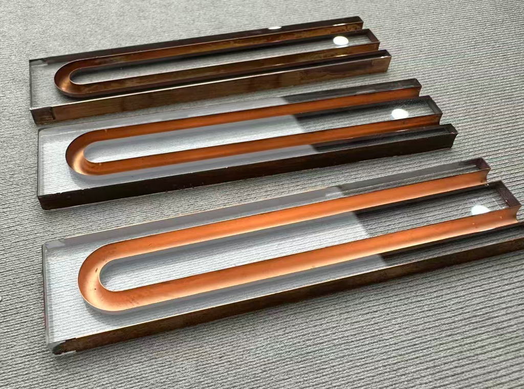
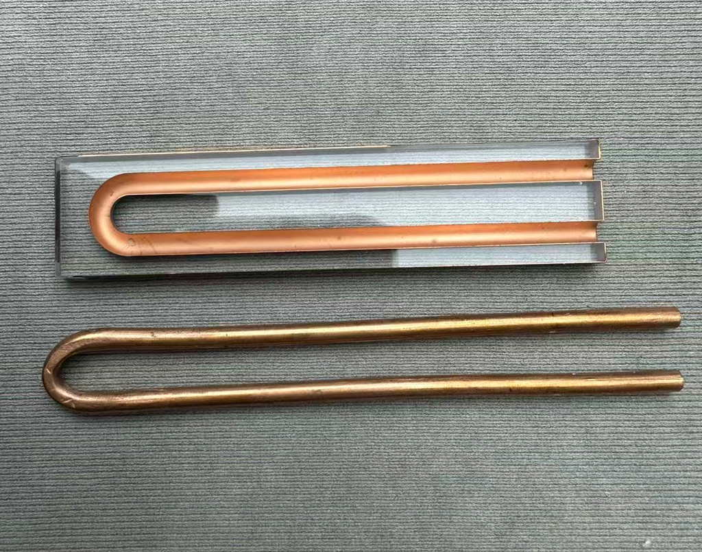
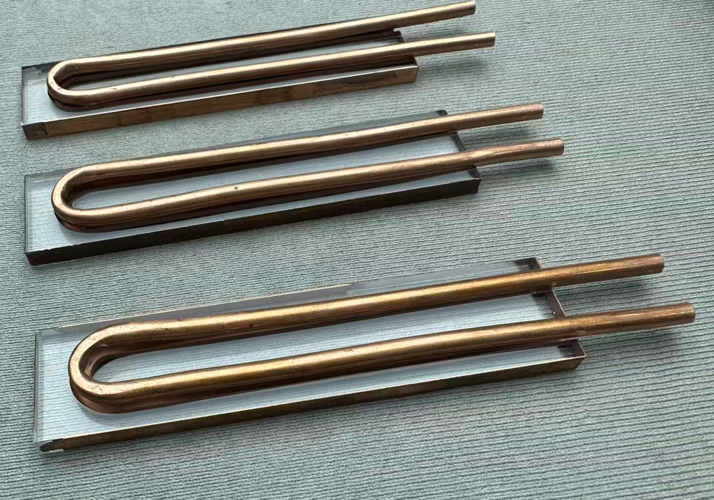
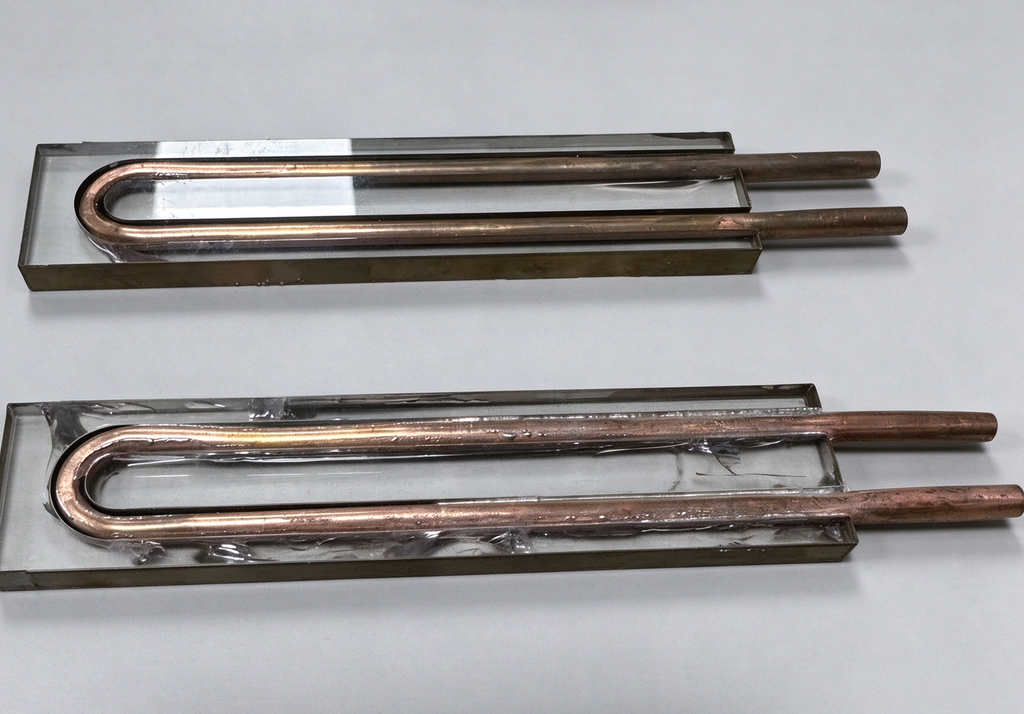
To address these pain points, KENFA TECH carries out joint R&D with SCHOTT. Based on them specialty glass, we retain the proven architecture: precision grooves are machined on their glass substrates, formed copper tubes are embedded inside the grooves, and thermal buffer TIM fills the gaps. The cold plate is placed at the optimal thermally coupled position near heat sources inside optical modules. Coolant flows inside copper tubes to remove heat. Glass serves as an insulating, low‑CTE substrate to resolve both issues above. Meanwhile, this design inherits mature copper tube routing, bending and joint sealing technology. No high‑cost glass fusion microchannel development is required. The copper tube forms an independent pressure‑resistant fluid channel with low leakage risk, suitable for rapid prototype verification. Unlike etched microchannel glass cold plates, copper tubing provides reliable pressure resistance.
2. Material Properties and Design Constraints of SCHOTT Glass Substrate Cold Plates with Embedded Copper Tubes
We use standardized SCHOTT specialty glass substrates. A comparison with conventional aluminum plates is shown below:
- Aluminum plate: thermal conductivity ~200 W/(m·K), ductile, stable under CNC machining, tolerates moderate clamping force; high CTE, electrically conductive, with inherent galvanic corrosion risks.
- SCHOTT fused silica glass: ultra‑low CTE (0.55 ppm/°C), best CTE match with silicon photonic chips for high‑end CPO applications; thermal conductivity only 1.4 W/(m·K), brittle, electrically insulating to cut off galvanic corrosion paths.
- SCHOTT borosilicate glass: good machinability with controlled cost, CTE ~3.3 ppm/°C, suitable for mid‑power pluggable high‑speed optical modules, also electrically insulating.
⚠️ Critical design note: Aluminum plates provide heat spreading in the original design. Glass has poor thermal conductivity and almost no heat spreading capability. Heat is mainly extracted by copper tubes adjacent to heat sources. Groove layout, copper tube arrangement and interface thermal resistance between copper tubes and glass grooves dominate thermal performance. Do not directly copy simulation parameters and heat‑spreading design rules from aluminum substrates.
The table below summarizes key performance differences between copper, aluminum and SCHOTT glass substrates for embedded copper tube cold plates, to support quick material selection for optical module thermal design.
| Item | Copper Substrate | Aluminum Substrate | SCHOTT Glass Substrate |
|---|---|---|---|
| Thermal Conductivity | ~401 W/(m·K) | ~200 W/(m·K) | ~1.4 W/(m·K) |
| CTE (Coefficient of Thermal Expansion) | 16.5 ppm/°C | 23.1 ppm/°C | 0.55 ~ 3.3 ppm/°C (Fused silica / Borosilicate) |
| Electrical property | Conductive | Conductive | Electrically insulating |
| Optical drift risk | HighLarge thermal deformation, easy to cause wavelength & insertion loss shift | HighLarge thermal deformation, optical coupling offset under temperature cycle | Very lowCTE matched with silicon photonic chips & optical waveguides |
| Galvanic corrosion risk | HighDissimilar metal contact + moisture/ion will form galvanic cell | Medium-HighSame corrosion mechanism as copper | Very lowInsulating substrate, no conductive corrosion loop |
| Machinability | Good, ductile, CNC easy; high cost | Excellent, easy CNC grooving, low cost | Brittle, requires ultrasonic / laser precision machining; risk of microcracks & chipping |
| Heat spreading capability | Excellent | Good | Almost none, heat transfer relies on embedded copper tubes |
| Allowable clamping pressure | High | High | Low, easy to crack under excessive compression |
| Outgassing & ionic precipitation | Low (with proper plating) | Low (with proper plating) | Low, compatible with optical cavity |
| Typical application scenario | Ultra-high heat flux, heat spreading required, no strict optical stability requirement | General high-power heat sink, cost-sensitive, no strict anti-corrosion & optical index | CPO / silicon photonic high-power optical modules, optical stability & anti-galvanic corrosion required |
| Main disadvantage | Heavy, high CTE, corrosion risk, high material cost | Medium CTE, conductive, corrosion risk | Poor thermal conductivity, brittle, high processing cost |
As shown in the table, their glass sacrifices heat spreading capability for ultra-low CTE and electrical insulation. This trade‑off effectively addresses optical drift and galvanic corrosion, which are the two dominant reliability risks for high‑power silicon photonic and CPO packages.
3. Common Icepak Simulation Pitfalls When Migrating from Aluminum to SCHOTT Glass Substrates
Many engineers reuse thermal simulation settings for aluminum designs, leading to 8–15 °C deviation between simulation and measurement. The five typical root causes are listed below:
- Incorrect material property assignment: glass treated as aluminum Using aluminum thermal conductivity overestimates lateral heat spreading of the substrate. Simulated chip temperature becomes artificially low and deviates strongly from physical testing. Glass cannot spread heat efficiently; hotspots remain if heat sources are far from copper tubes.
- Ignored interface thermal resistance between grooves and copper tubes Aluminum grooves can achieve tight contact with controllable interface resistance. After machining, their glass grooves have minor chipping and surface roughness. TIM fills the gaps between copper tubes and glass. This interface accounts for a large share of total thermal resistance. Bonding faces directly in simulation without TIM layers will greatly underestimate thermal resistance.
- Missing thermal‑structural coupling evaluation Aluminum is ductile and can release stress from assembly clamping and temperature variation. Glass is brittle. Its glass, copper tubes and TIM have different CTE values. Temperature cycling creates local stress concentration, which may crack the glass or squeeze optical coupling regions. Temperature‑only simulation without thermal‑structural coupling leaves reliability risks.
Note: This stress originates from CTE mismatch between copper tubes and glass. It differs from bulk deformation of metal substrates that shifts the whole optical path and is more controllable.
- Over‑simplified geometry by removing groove fillets and machining chipping the glass grooves are usually fabricated by laser processing or ultrasonic milling. Corners have fillets and minor edge chipping. Simplifying grooves to ideal rectangles changes TIM thickness and contact area, resulting in incorrect thermal resistance calculation. Minor chipping has negligible thermal impact on aluminum designs but cannot be ignored for glass substrates.
- Unreasonable clamping load boundary inherited from aluminum designs Higher clamping force reduces interface resistance for aluminum cold plates. the glass cannot sustain high clamping pressure and may crack under excessive load. Simulation using aluminum clamping assumptions yields ideal low thermal resistance, while actual assembly pressure is limited and thermal resistance rises.
The table below compares reliability performance and operating limits for the three substrate options under typical optical module qualification conditions.
| Item | Copper Substrate | Aluminum Substrate | SCHOTT Glass Substrate |
|---|---|---|---|
| Max continuous operating temperature | 180 °C | 120 °C | 150 °C (Borosilicate) / 1000 °C+ (Fused silica) |
| Thermal cycling resistance (-40 ~ 125 °C) | Excellent, ductile, resistant to thermal fatigue | Good, risk of TIM delamination under long cycles | Good, low CTE mismatch with optics; risk of cracking if clamping stress is excessive |
| 85°C / 85%RH damp heat test | Risk of galvanic corrosion with dissimilar metals | Risk of galvanic corrosion with dissimilar metals | Very low corrosion risk, insulating substrate |
| Max working pressure for embedded copper tube | High | High | Medium (limitation comes from glass substrate, not copper tube) |
| Sensitivity to ionic contaminants / flux residue | High | High | Low |
| Compatibility with optical cavity low-outgassing specs | Acceptable after plating | Acceptable after plating | Excellent |
| Risk of short circuit to PCB / photonic die | High (conductive) | High (conductive) | None (insulating) |
| Vibration & shock performance | Excellent | Excellent | Medium, brittle, needs proper fixture design |
Glass removes electrical short and galvanic corrosion risks, but engineers must control clamping stress and shock loads in mechanical design.
4. Manufacturing Process Specifications of KENFA TECH × SCHOTT Glass Cold Plates with Embedded Copper Tubes
Process flow: Original the glass substrate → precision grooving by ultrasonic or laser milling → groove cleaning → copper tube bending → copper tube embedding → gap filling with low‑ion thermal buffer material → curing → fluid joint sealing → thermal resistance, pressure and insulation testing
- Glass grooving: ultrasonic milling is preferred for controlled edge chipping. Laser grooving delivers high speed but may introduce microcracks, which require dedicated the glass polishing to eliminate defects.
- Copper tube selection: oxygen‑free copper tubes are standard, nickel plating is available upon request to protect copper from corrosion and isolate base copper from fillers and moisture.
- Gap filling: thermal gel or thermal epoxy balances thermal conduction and stress buffering. It absorbs CTE mismatch strain between copper tubes and the glass to prevent cracking during temperature cycling. Selected fillers feature low ionic content and low outgassing to avoid optical surface contamination.
- Fluid sealing: copper tubes form independent flow channels. Only end connectors require sealing. Compared with fusion‑bonded glass microchannels, leakage risk is much lower and prototyping cycle is shorter.
Comparison of two architectures
✅ Aluminum plate with embedded copper tubes: good heat spreading, low cost, high clamping tolerance. Drawbacks: large CTE mismatch, obvious optical drift at high power, conductive base with galvanic corrosion risk. ✅ the glass plate with embedded copper tubes: low CTE, insulating substrate to eliminate galvanic cells, superior optical stability, reliable pressure resistance and fast prototyping. Drawbacks: no heat spreading, brittle material, higher processing cost.
5. Application Selection Guideline
This SCHOTT glass cold plate with embedded copper tubes is recommended for these scenarios:
- CPO and silicon photonic high‑power optical modules requiring stable wavelength and insertion loss, with strict control of thermally induced optical shift;
- Packages with residual moisture or ionic contaminants, where galvanic corrosion and leakage must be avoided;
- Projects that want to adopt proven embedded copper tube flow architecture without high investment in glass microchannel bonding development;
- Fast prototype validation, requiring pressure‑resistant flow channels with low leakage probability;
- Optical cavity environments where heavy outgassing from organic adhesives is prohibited.
Not recommended for:
- Large areas with scattered heat sources that demand substrate‑level heat spreading;
- Ultrahigh heat flux applications with heat sources widely separated from copper tubes;
- Cost‑sensitive projects without optical stability or corrosion control requirements.
The table below outlines simulation workload and risk differences when building Icepak models for these three substrates.
| Item | Copper Substrate | Aluminum Substrate | SCHOTT Glass Substrate |
|---|---|---|---|
| Required simulation type | Thermal only | Thermal only | Thermal + structural coupling |
| Ease of geometry simplification | Easy | Easy | Hard, cannot ignore micro chipping and fillets |
| Interface thermal resistance sensitivity | Low | Low | High |
| Material parameter sensitivity | Low | Low | High (thermal conductivity stable, but stress highly CTE dependent) |
| Risk of simulation-to-test deviation | Low | Low | High if model simplified improperly |
Extra care is required for glass substrate simulation. Over-simplification will create large temperature gaps between simulation and measured data.
6. Validation Test Suite
Our validation covers not only junction temperature measurement. Four groups of tests are performed for this brittle glass optical thermal solution:
- Thermal performance test: flow rate vs pressure drop curve, junction temperature and thermal resistance characterization;
- Temperature cycling durability test: verify stress release among copper tubes, filler and SCHOTT glass, confirm no cracking or leakage;
- Synchronized optical monitoring: track insertion loss and wavelength shift under temperature cycling, benchmark against metal cold plates;
- Corrosion reliability test: accelerated aging under 85 °C / 85 % RH ionic environment to verify galvanic corrosion suppression by the insulating substrate.
What can Kenfa tech help for your thermal project?
This article shares practical R&D experience from the joint development program between KENFA TECH and SCHOTT for high‑power optical modules. Based on your optical layout drawings and power specifications, we can complete copper tube routing simulation, groove process assessment, sample fabrication and benchmark testing.
If you have alternative ideas or design proposals, please email us for discussion: king@kenfatech.com